Quick Links
Home > PCB Assembly > PCB Assembly Services > Through-Hole Assembly
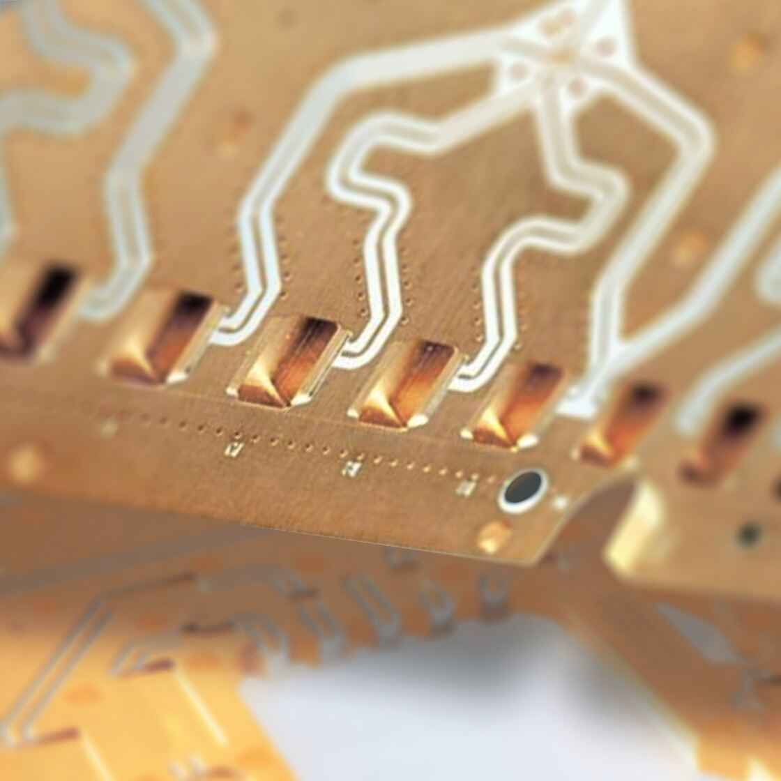
Through-hole PCB assembly is a classic method for mounting electronic components. Its operation is straightforward: component leads are inserted through pre-drilled holes in the PCB board and then soldered in from both sides to create a conductive path. Hand soldering is suitable for small batches or delicate work, while wave soldering is more commonly used in mass production. Both methods ensure a secure connection between components and the PCB.
In the early days, electronic devices primarily relied on single- and double-layer PCBs, and through-hole assembly was the mainstream technology. Later, with the prevalence of multi-layer boards, surface mount technology (SMT) gradually became mainstream due to its high density and miniaturization. After all, through-hole components and drilled holes take up more space, making them difficult to meet the design requirements of delicate devices. However, this does not mean that through-hole assembly will be eliminated: although some predicted its demise in the 1980s, it still plays a role in many applications today, often even used in conjunction with SMT. Large industrial equipment and high-power devices are particularly dependent on it. Firstly, it is much easier to disassemble and repair damaged components than SMT. Secondly, its structure can withstand harsh environments such as high temperature and vibration.
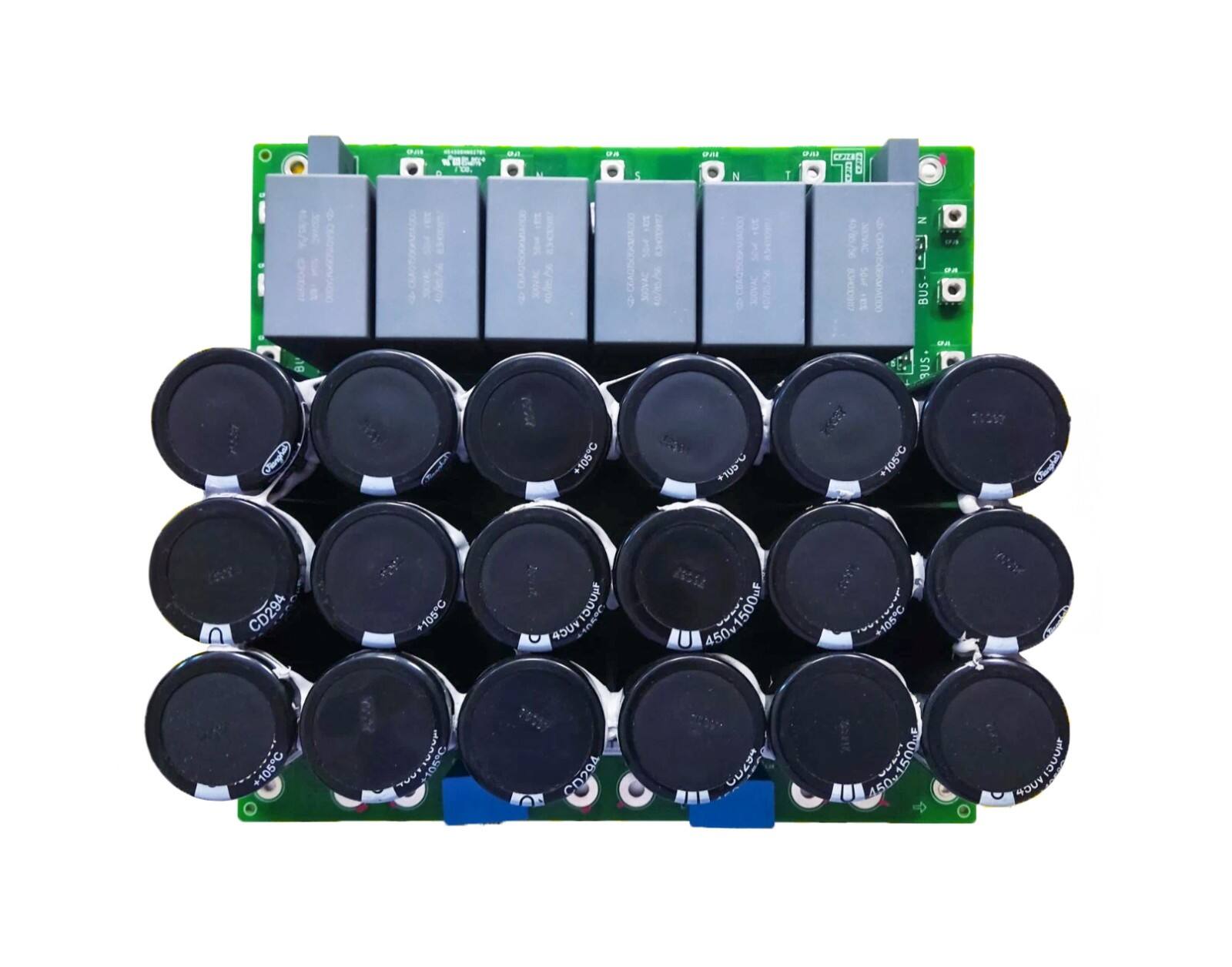
1. Suitable for High-Power and Large Components: High-power resistors and large connectors used in industrial equipment are both bulky and carry large currents. Through-hole assembly securely holds these components, meeting the demands of high-power scenarios.
2. Stable Connections and Environmental Resistance: Component pins pass through the PCB and are soldered on both sides, creating a connection with high mechanical strength that withstands environmental stresses such as vibration and temperature fluctuations, ensuring reliable performance in complex environments like automotive and industrial applications.
3. Excellent Heat Dissipation Efficiency: Large components paired with through-hole assembly allow heat to be quickly transferred to the PCB through the pins and solder joints, making it suitable for applications requiring efficient heat dissipation, such as power electronics.
4. Easy Maintenance: Damaged components can be removed and replaced simply by melting the solder joints with a soldering iron, eliminating the need for complex equipment. This is particularly suitable for equipment requiring frequent maintenance.
1. Limited Circuit Density: Through-holes and the components themselves occupy a large amount of space, limiting the number of components that can be mounted on a PCB. This makes it unsuitable for high-density designs such as mobile phones and chipsets.
2. Disadvantages to Miniaturization: Through-hole components are larger than SMT components, and the need for drilling increases the weight and thickness of the PCB, making it incompatible with lightweight requirements for portable devices.
3. Production Efficiency and Cost Disadvantages: Many through-hole components require manual insertion, which slows down mass production. Compared to SMT's automated process, through-hole components are more time-consuming and costly.
The entire process consists of three steps, each closely linked to ensure quality:
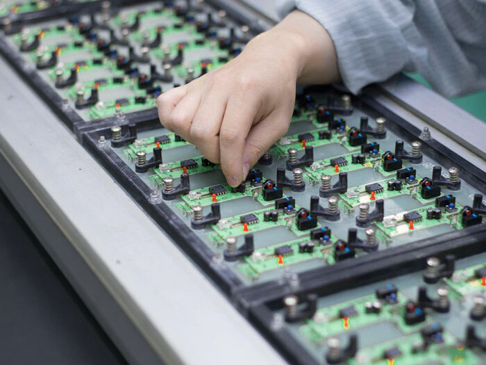
The first step is component insertion: A worker or semi-automatic equipment inserts components with leads, such as resistors and diodes, into pre-drilled holes on the PCB according to the design requirements, ensuring that the leads extend the appropriate length from the back of the board, preparing for soldering.
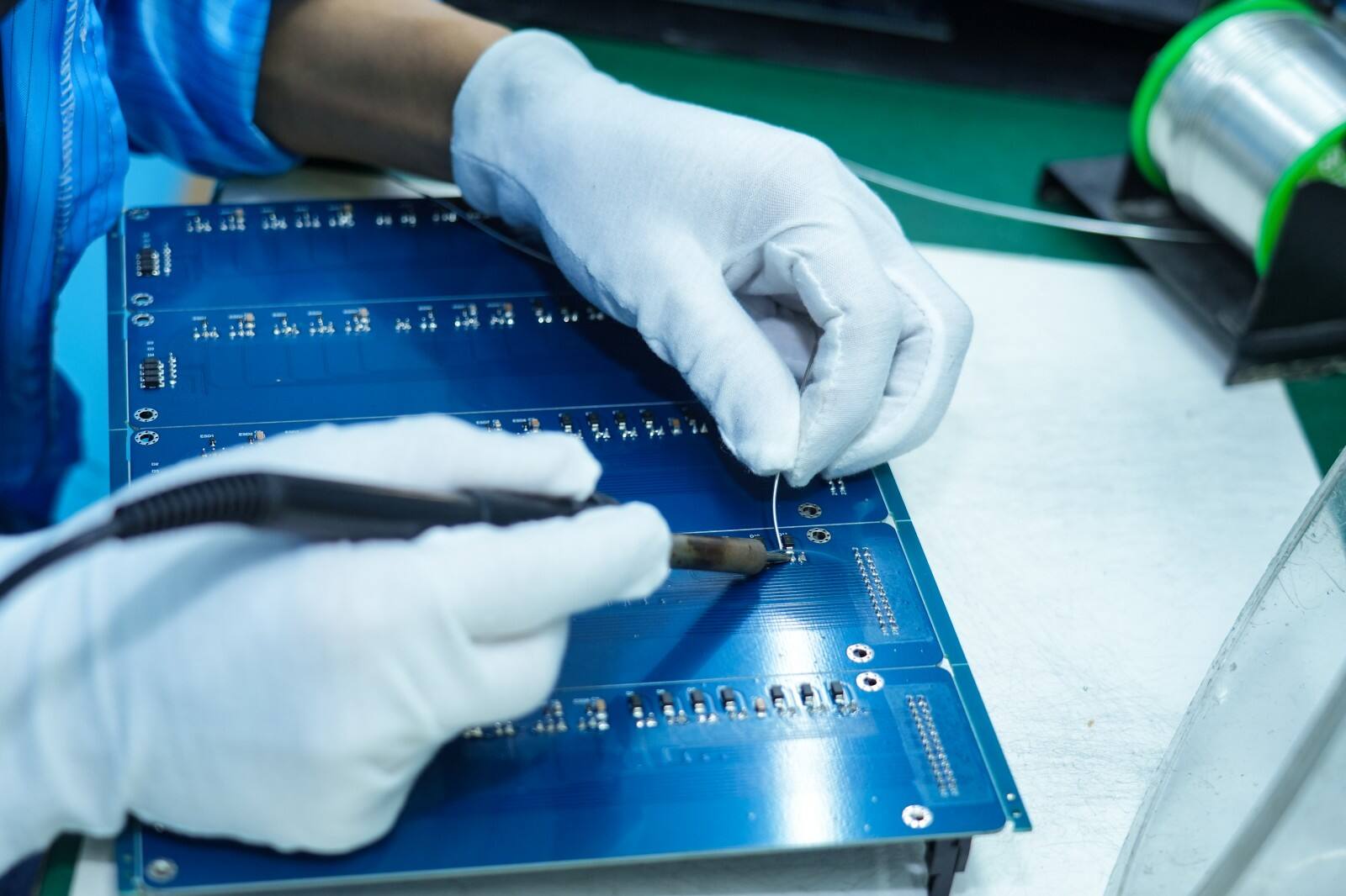
The second step is soldering and securing: After the components are inserted, solder (a low-melting-point metal alloy) connects the leads to the PCB pads, creating a conductive path. Wave soldering is commonly used in mass production—the PCB is passed through a wave of molten solder on a conveyor, completing back-side soldering in one operation. For components sensitive to high temperatures, selective soldering is used to precisely apply hot solder to the target solder joints to avoid affecting other components.
The third step is cleaning: After soldering, residual flux must be removed with a solvent and a brush to prevent it from corroding the PCB or causing electrical interference, ensuring long-term stability.
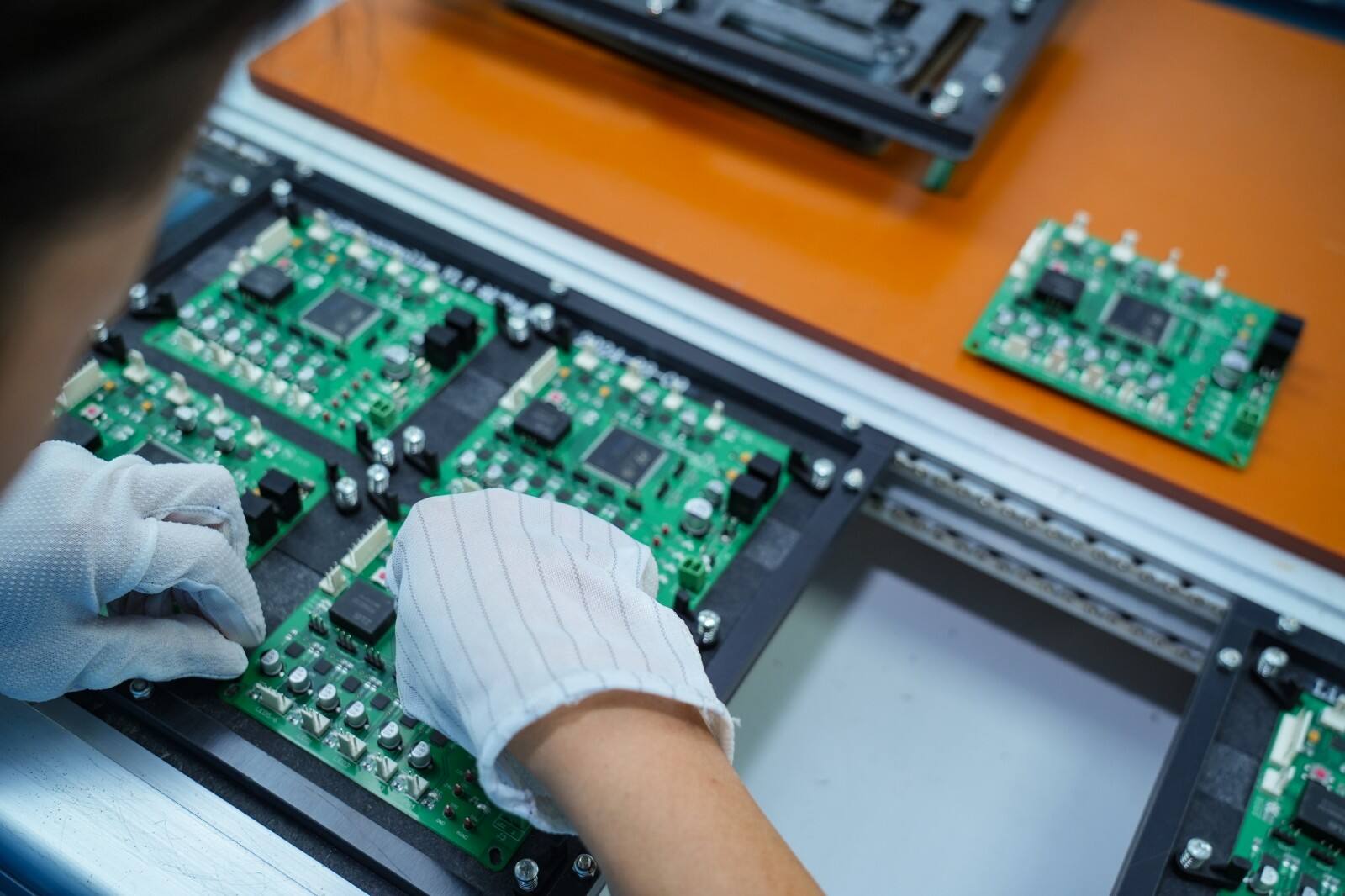
1. We provide a full-process service from component procurement to finished product testing, covering processes such as single- and double-sided hand soldering and wave soldering. Whether it's standard components like resistors and connectors, or through-hole devices with specialized specifications, we ensure precise assembly.
2. For quality control, we use automated optical inspection (AOI) to inspect solder joint appearance, in-circuit testing (ICT) to verify circuit continuity, and finally, functional testing to ensure product performance meets standards. We also support mixed through-hole and SMT assembly, flexibly meeting diverse needs from small-batch trial production to large-scale production.
3. With advanced equipment, an experienced technical team, and a strict quality management system, we have provided stable services to various industries, including automotive, industrial, and medical. Whether you need a small-batch prototype verification or a long-term mass production supplier, you can find reliable support here.
If you're unsure about the assembly method for your project, please contact PCBally. We will provide professional advice based on your product characteristics, ensuring that each PCB performs optimally with the appropriate process.
HDI PCB
Through-Hole Assembly
Copper Based PCB
Teflon PCB