Quick Links

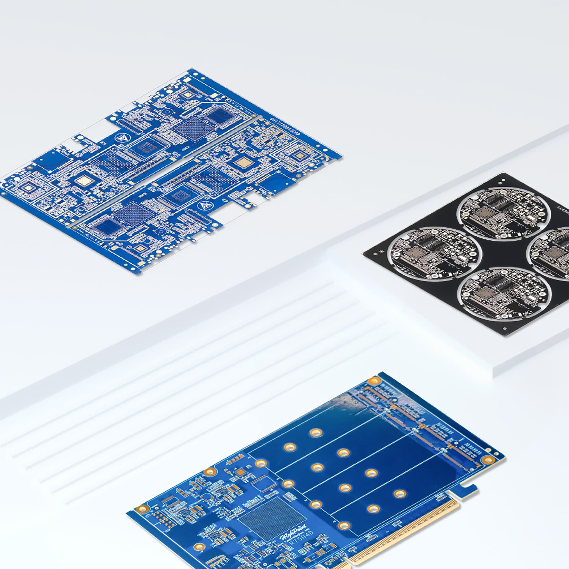
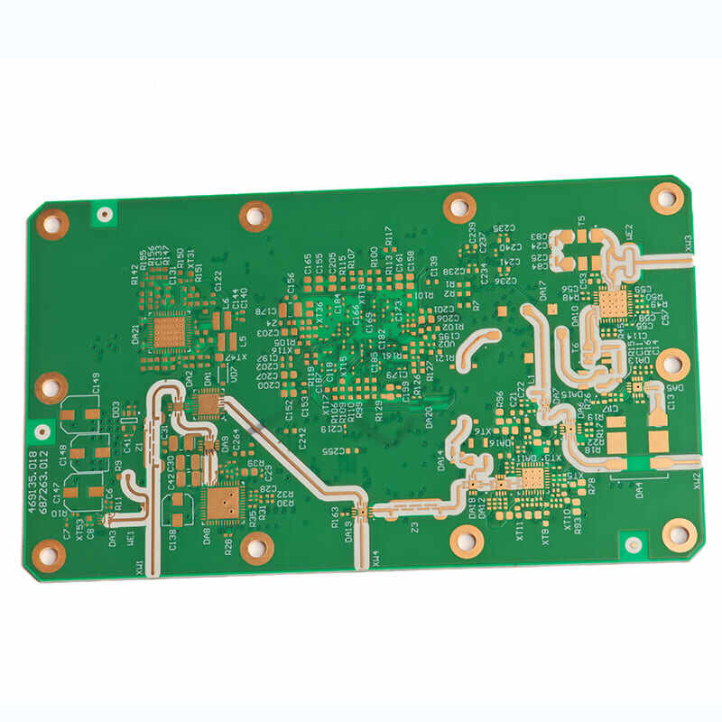
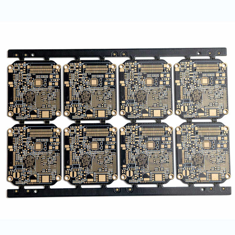
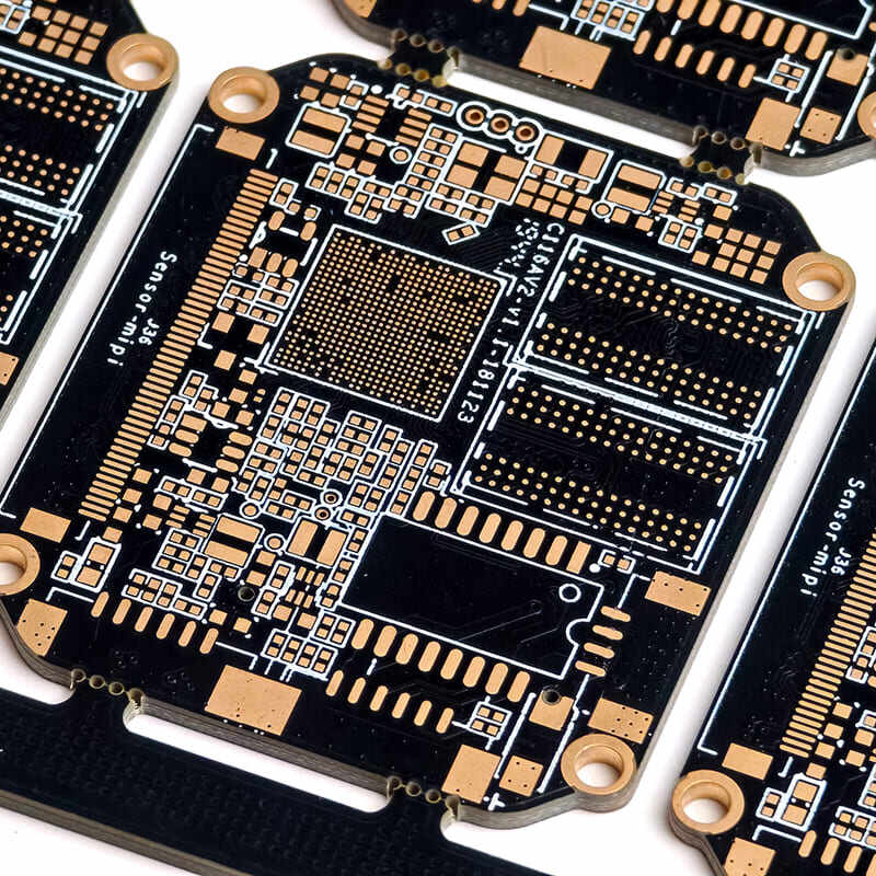
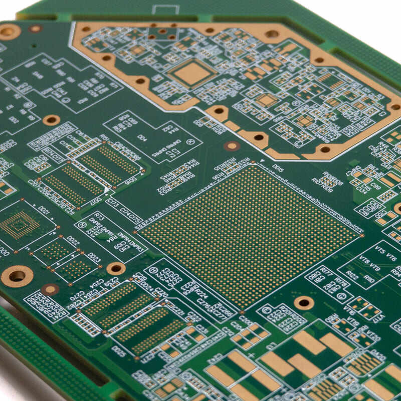
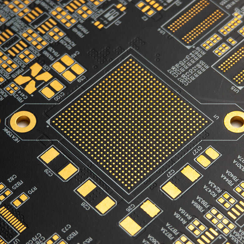
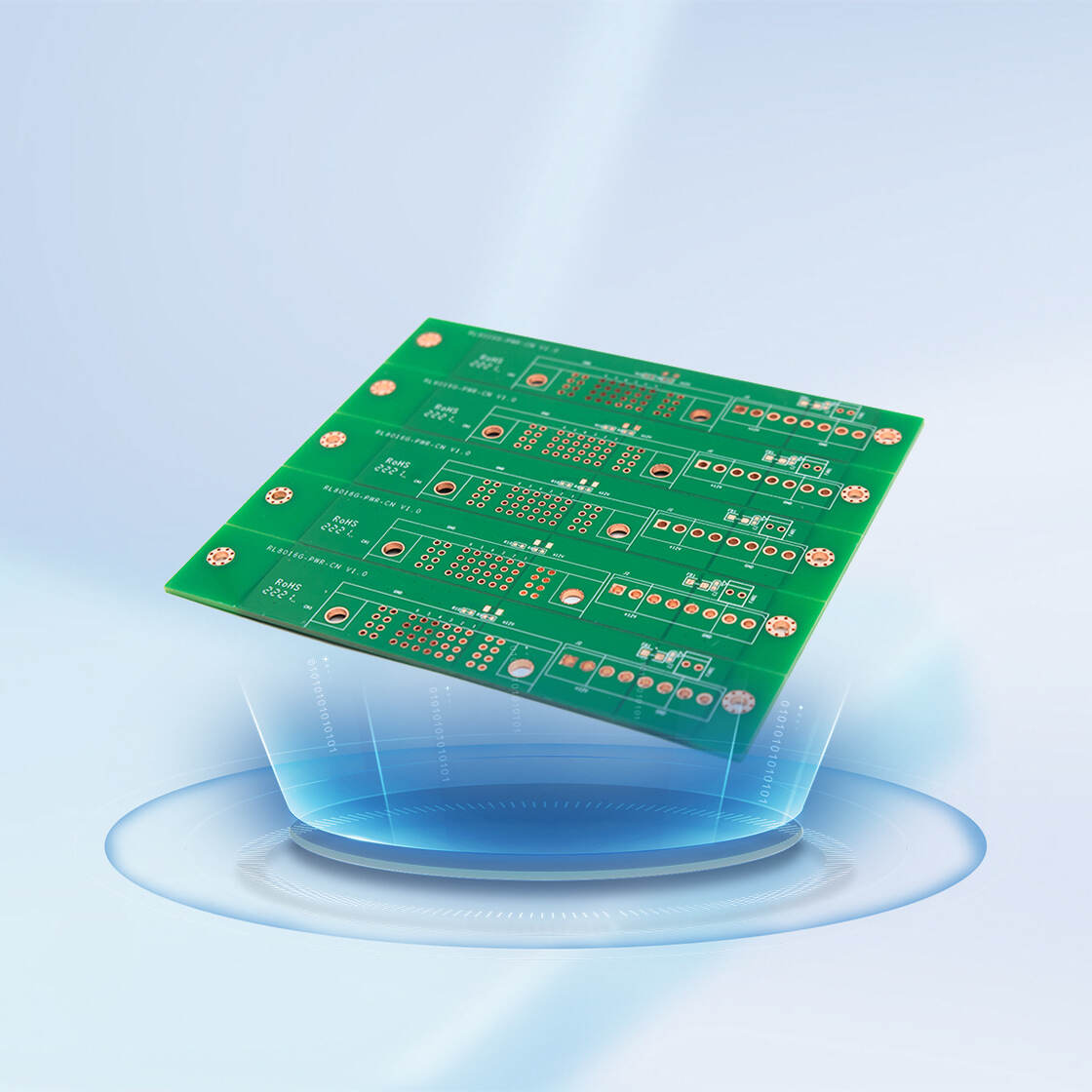
HDI PCB is the abbreviation of High-Density Interconnect Printed Circuit Board. As its name suggests, this is an advanced PCB designed to meet the miniaturization and high-performance requirements of electronic products. High-density PCB is characterized by fine lines and fine hole pitch. Compared with traditional PCB, high-density PCB optimizes wiring density by reducing lines, abandons traditional through-hole (Through Hole Via) process, adopts laser drilling such as micro vias (Micro Via), blind vias (Blind Via) and buried vias (Buried Via), and lamination technology, to achieve circuit integration far exceeding traditional PCB, can accommodate more components per unit area, can realize more complex circuit functions in a limited space, and allow electronic products to carry stronger performance in a smaller volume, thus accurately adapting to the era of electronic products towards lightweight, intelligent, and high-frequency development needs, and becoming a key carrier to support breakthroughs in emerging fields such as 5G, Internet of Things, and artificial intelligence.
With its unique design and process, high density interconnect pcb shows a series of core features that adapt to high density and high performance needs, mainly including:
HDI circuit boards usually have higher number of layers, usually more than 4 layers. This is because it is difficult to avoid line congestion and signal interference with only a few layers, so it is necessary to increase the number of layers and distribute the wiring and connections to multiple layers for reasonable planning. Most products will choose a 6 to 12-layer design based on the complexity of the function to balance the wiring density, functional complexity and circuit performance in a limited space.
In order to meet the needs of miniaturization of electronic devices and achieve higher density circuit integration in a limited space, hdi circuit board must distribute lines efficiently. hdi circuit board can achieve 3-5mil or even smaller line width and line spacing, while the wiring spacing of traditional circuit boards is usually several hundred microns. Therefore, when manufacturing hdi printed circuit board, any slight process deviation will cause line deformation, short circuit or open circuit, which is extremely difficult to process.
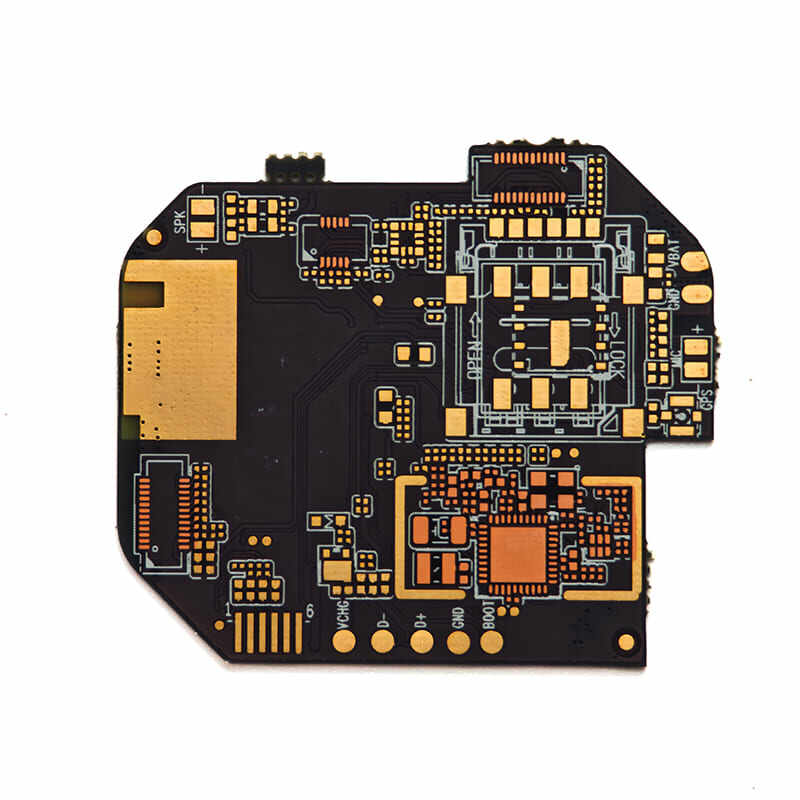
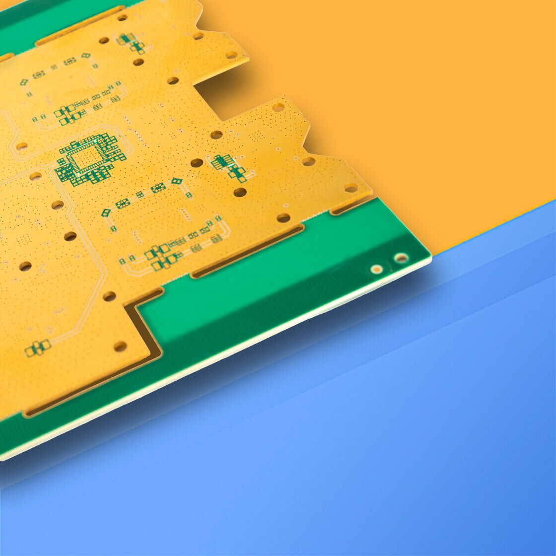
The hole design in HDI boards is also very fine. The hole types include: Microvia, which usually has a hole diameter of less than 6mil, so as to accurately connect fine lines and save space. In order to achieve connections between multiple layers, it is often necessary to stack them up layer by layer, and the holes usually need to be filled with copper or electroplated; Blind Via, which extends from the surface layer to a specific internal layer and is only visible on one side. It is achieved through a segmented drilling process, which effectively shortens the signal path and reduces interlayer interference; Buried Via, which is completely embedded in the inner layer and does not penetrate the surface layer. It needs to be manufactured through a multi-stage lamination process, which can release the surface wiring space and enhance the integrity of the inner power/ground plane; Staggered Via, which is composed of multiple staggered microvias to form a staircase interconnection structure, which is suitable for scenarios where cross-layer connections are required but space is limited; Stacked Via, where multiple layers of microvias are vertically stacked to form a columnar structure, to achieve multi-layer direct interconnection, but the drilling accuracy needs to be strictly controlled to ensure electrical reliability. The reasonable combination and application of these hole types can meet the design requirements of high-density and high-performance PCBs.
In order to make the wiring more dense, HDI will also use VIP technology, that is, directly drilling microholes in the pads and connecting them with thin lines, thereby widening the wiring channel and solving the problem of line congestion in high-density scenarios. According to the spatial position relationship between the pads and holes, it can be subdivided into the following types:
The hole structure layout of HDI PCB needs to meet the requirements of high-density interconnection and signal integrity. During manufacturing, it is necessary to precisely control the inter-layer alignment accuracy (within ±15μm) to achieve a low aspect ratio of ≤1:3 to ensure stable signal transmission; the core layer uses a thicker substrate, and the buried hole design can enhance the electrical connectivity of the middle layer to better meet the application requirements of high-density, high-performance electronic devices.
HDI PCB exhibits unique characteristics in stacking and lamination process:
Although it uses layer-by-layer construction logic like traditional PCB, multiple rounds of stacking and lamination processes are required to achieve complex interconnection designs of multi-layer blind and buried vias. Its structure is based on a thick core layer, with thin dielectric layers symmetrically laid on both sides to form an infrastructure suitable for high-density wiring.
The specific manufacturing process is: first define the conductive area with a negative photoresist film, and use ferric chloride to etch away unnecessary parts; then use a chemical solution to remove the photoresist film to expose the substrate to be processed; the drilling process selects mechanical, laser or chemical methods according to density requirements; then the inner layer circuit interconnection is completed through the metallization process; finally, the stacking and plating operations are repeated until the outer layer structure is formed, so as to meet the precision interconnection requirements in high-density scenarios.
Feature |
Capability |
| Quality Grade | Standard IPC 2 |
| Number of Layers | 4-32 layers |
| Line Width/Line Spacing | 1.5~2mil(0.035~0.05mm) |
| Minimum Mechanical Drilling | 0.2mm |
| Minimum Laser Drilling | 0.1mm |
| Blind/Buried Vias | 0.1~0.2mm |
| Via Hole (PTH) | ≥0.3mm |
| Via Aperture Ratio | 8mil(0.2mm) |
| Line Spacing/Pad Spacing | 3mil(0.075mm) |
| Minimum Pad Size | 0.15~0.4mm |
| Solder Mask Spacing | ≥3mil (0.075mm) |
| Solder Mask Color | Green, White, Blue, Black, Red, Yellow, Purple |
| Plate Thickness | 0.4~1.6mm |
| Materials | High Tg FR4, Nelco N7000-2 HT, Isola I-Speed and other low-loss materials |
| Stacking Method | Sequential Lamination |
| Micropore Filling | Resin filling/Electroplating filling |
| Metal Layer Thickness | 1oz-2oz(35μm-70μm) |
| Minimum Hole Spacing | ≥0.2mm |
HDI PCB (high-density interconnect printed circuit board) has shown significant advantages in the trend of miniaturization and high performance of electronic equipment with its unique design and process, which is mainly reflected in the following aspects:
Through precision technology, HDI can achieve massive line connections in a limited area. Compared with traditional PCB, it can reduce the volume by 30%-50% under the same function, while reducing the weight of the equipment, providing a space and lightweight foundation for the equipment.
Although the manufacturing cost of hdi board is relatively high, by reducing the number of components, optimizing space utilization and simplifying the assembly process, the design and manufacturing cost of the overall system can be significantly reduced, and the long-term cost performance is better.
The multi-layer process supports 6-12 layers or even more layers. Combined with structures such as stepped holes and stacked holes, complex circuit topologies can be flexibly planned.
Short and straight signal paths reduce parasitic inductance and capacitance, effectively control noise, and reduce signal transmission delay and loss; the multi-layer structure can separate the power supply, ground and signal layers to reduce electromagnetic interference (EMI).
Adapting to the rapid development and testing process of compact equipment, its high integration and design flexibility can shorten the cycle from prototype to mass production, helping products respond to market demand faster.
Although aluminum-based PCBs have many advantages, they still have some disadvantages:
Portable devices such as smartphones, tablets, smart watches, and products such as augmented reality (AR) and virtual reality (VR) need to integrate high-resolution displays, sensors, processors and other components in a small space. HDI's high-density interconnection capability can meet their compact design and high-performance requirements;
Autopilot systems, in-vehicle infotainment systems, etc. need to achieve high-speed wiring of high-speed processors and RAM in the limited space of the vehicle, meet the requirements of low crosstalk, high compatibility and signal integrity, and adapt to multi-sensor data interaction and high-speed computing scenarios;
5G base stations, routers, satellite communication terminals, etc., rely on HDI to optimize high-frequency signal transmission, reduce delays and interference, and support high-bandwidth data interaction;
Portable monitors, ultrasound equipment, minimally invasive surgical robots, capsule endoscopes, etc. require miniaturized design and precise signal control. HDI can balance volume and performance while meeting high safety standards and operating accuracy requirements;
Military and aerospace equipment such as drones, satellite payloads, and radar systems integrate high-power and high-sensitivity components, and have extremely high requirements for data accuracy, communication reliability, and lightweight. HDI's lightweight structure and reliable interconnection technology can meet performance requirements in extreme environments;
The control systems of precision CNC machine tools and industrial robots require high-density wiring to support multi-axis linkage signal transmission. HDI can improve the response speed and operation stability of the equipment.
Although the design of HDI circuit boards can meet the requirements of high density and high performance, it also faces multiple technical challenges, which are mainly reflected in the following aspects:
1. The adaptability of design and manufacturing, which must strictly follow the design for manufacturability (DFM) guidelines to ensure that the design can match the production capacity;
2. The planning of the number of layers, which usually refers to the recommended standards of BGA devices, or is based on the comprehensive judgment of the direction and length of the cross-network, laying the foundation for subsequent design;
3. The design of the hole structure, the distribution of the holes will directly affect the reasonable setting of the thickness and number of layers of the board, and is the key to connecting the lines of each layer;
4. Assembly reliability and environmental adaptability, it is necessary to ensure that the circuit board will not break during use, and take into account durability and stability;
5. The technical strength of the manufacturer, whose process level is directly related to the manufacturability of the entire board, the wiring quality and the final operation effect.
For high-density interconnected PCBs, their production, manufacturing and design links need to be strictly implemented in accordance with a series of standards formulated by IPC, including IPC-2315, IPC-2226, IPC-4104 and IPC-6016.
There are many differences between the manufacturing of HDI PCB and standard PCB, and its limitations are mainly reflected in the compatibility of materials and processes:
1. The substrate must meet the requirements of both electrical and mechanical properties, and the dielectric material must be compatible with high TG values, thermal shock and metal welding, and must be compatible with various hole types such as microvias, buried vias, and blind vias;
2. The adhesion and performance stability of copper foil in areas such as microvias and buried vias must be reliable;
In addition, the material must have good thermal stability to withstand the impact during welding or thermal cycling.
The relevant standards are IPC-4101B and IPC-4104A, involving materials such as photosensitive liquid dielectric layer, dry film dielectric layer, polyimide film, thermosetting film, resin-clad copper foil, and standard FR-4.
In the booming global HDI circuit board industry, China has become a key manufacturing center, and many high-quality manufacturers have emerged, among which PCBally is a leader. With its profound accumulation and innovative strength, PCBally has demonstrated significant advantages in many aspects:
Rogers PCB
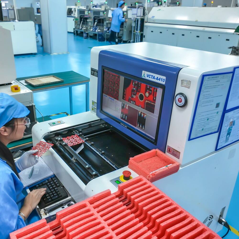
A.O.I.
Annular Rings
Gold Finger PCB