Quick Links

In PCB design and manufacturing, vias are used as "bridges" to connect different layers. If they are exposed, they can easily become a hidden danger that affects the quality of assembly. During soldering, solder paste may fall into the hole, resulting in insufficient solder joints or even failure to form effective solder joints, just like a gap in a dam will leak water. Once such problems occur, they will directly affect the conductivity and reliability of the circuit.
Via covering technology, in simple terms, is to wrap or fill the vias with a solder mask or special materials, which can effectively prevent solder paste from penetrating and reduce the risk of accidental short circuits. According to the functional requirements and application scenarios of vias, there are three common covering methods:
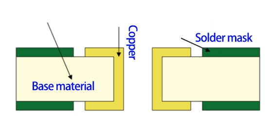
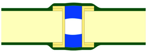
Via Tenting directly covers the vias with solder mask ink without additional process steps, just like covering the vias with a layer of "gauze". There are two specific forms:
1. Single-sided shielding: one side of the via is covered with solder mask ink, and the other side remains open, which is suitable for scenarios with slight heat dissipation requirements;
2. Double-sided shielding: both sides of the via are completely covered with solder mask ink, which is more protective and suitable for ordinary signal vias, and can effectively prevent solder paste from flowing into the hole by mistake.
This method is low-cost and simple in process, and is the most widely used basic protection method in conventional PCBs. Note when designing: The solder mask layer window opening file must clearly mark the area that does not need to be covered to avoid conflicts between the shielding process and design requirements
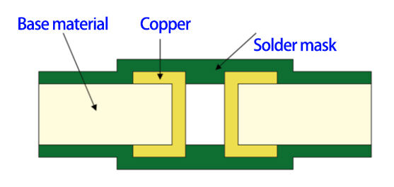
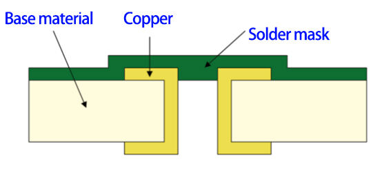
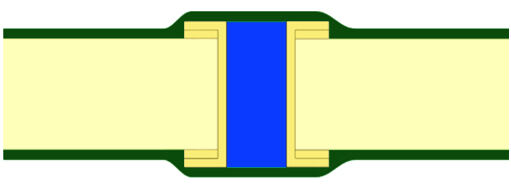
Via Plugging is to "half-fill" the via with non-conductive materials such as epoxy resin and solder mask ink, just like plugging the via with a "soft plug". There are two specific methods:
1. Single-sided plugging: partially fill the via with non-conductive material from one side, cover the surface with solder mask, and keep the other side open;
2. Double-sided plugging: partially fill both sides of the via and cover with solder mask.
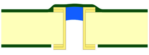
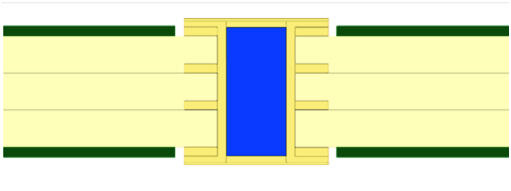
Via filling is to fill the via completely with non-conductive material, which is equivalent to adding a "solid core" to the via. This process is particularly suitable for high-density layout areas such as BGA. If the vias in these places are exposed, the solder paste will flow from the pad into the hole during welding, resulting in insufficient solder joints to form cold solder joints, or even no soldering at all, which has a great impact on the assembly quality of the PCB. Its main forms are:
1. Full filling + optional coverage: fill the via completely with non-conductive material, and the surface can be covered with solder mask (or not covered, depending on welding requirements);
2. Filling + Capping: This is a more sophisticated process - first electroplate and clean the via, then press in non-conductive material and solidify it, and finally grind the end face of the hole flat and metallize it to make the surface both flat and solderable. This method is particularly suitable for "Via-in-Pad" design, and can also support stacked micro via packaging, clearing the way for dense wiring between BGAs.
Choosing the right via coverage method requires a comprehensive judgment based on factors such as via diameter, number of PCB layers, and assembly requirements. Whether it is basic shielding or advanced filling, the core is to reduce welding risks and improve PCB reliability. This is also the principle we always adhere to in process selection to ensure that every PCB can withstand the test of actual application.
Via Covering
Through-Hole Assembly
Fr4
Plated Half-holes