Quick Links
Home > PCB Manufacturing > Drills & Throughplating > Plated-through Slots
A plated through slot (PTS) is a slot on a PCB (printed circuit board) that is plated with conductive material. It is used to achieve electrical connections between different layers of the PCB. I will introduce the plated through slot from four aspects: definition, advantages, design considerations, and manufacturing process.
Electroplating slots refer to long slots that have been treated with copper electroplating. They can be used for electrical connections and are an effective way to achieve copper plating on PCB through holes. Electroplating slots belong to the electroplating process inside the PCB, while the electroplating on the outer edge of the PCB is called edge plating.
Slots can be defined as plated through holes (PTH) or non-plated through holes (NPTH). When the milling slot connects the upper and lower copper layers, it forms a plated through hole (PTH). Plated through slots are often used for pin connections of through-hole packaged devices, and both plated through slots and non-plated through slots can be used in PCBs at the same time.

Plated through slots provide a better fit than standard round holes for mounting components with rectangular leads. Benefits include:
During the design phase, the length and width of each plated through-slot must be accurately marked and described in the manufacturing drawings to help manufacturers clarify processing requirements.
In EDA design tools, you can define plated through slots by adding elliptical holes. You can also define these slots in the mechanical layer of the Gerber file. If the design file does not include a mechanical layer, you can add a mechanical layer and define the slots there.
In addition, it is recommended to include a README file that clearly documents the design requirements for the plating through-well to ensure accurate communication.
The minimum width of the plated through slot provided by PCBally is 0.5mm, and the minimum width of the non-plated through slot is 0.8mm.
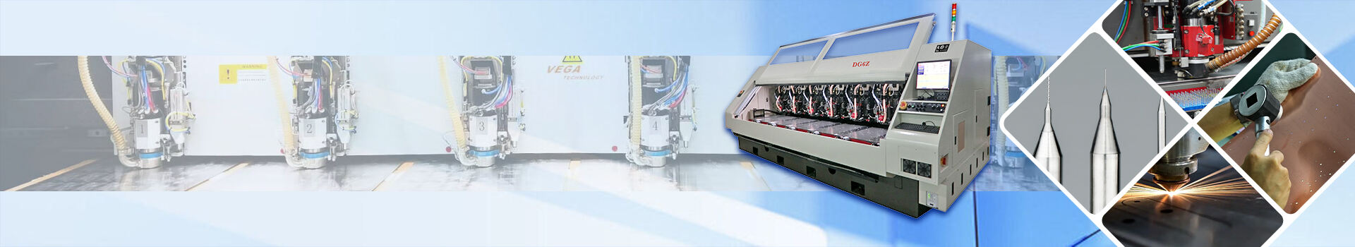
1. Milling: Use a milling cutter to mill slots of the required size on the PCB material, and remove the excess copper layer on the surface to form pads, traces and other structures;
2. Drilling cleaning: Clean the slots according to design requirements and remove residues;
3. Chemical copper plating: Use the same chemical copper plating process as through-hole electroplating to electroplate the inner wall of the slot to ensure that it has excellent conductivity;
4. Surface treatment: Perform subsequent surface treatment processes such as immersion gold and tin spraying according to requirements.
Generally speaking, when dealing with through-hole devices with rectangular or non-standard pins, if round through-holes are still used, extra space will be left in the hole. In order to avoid this problem, we should customize the slots that match the shape of the component pins to achieve a better fit.
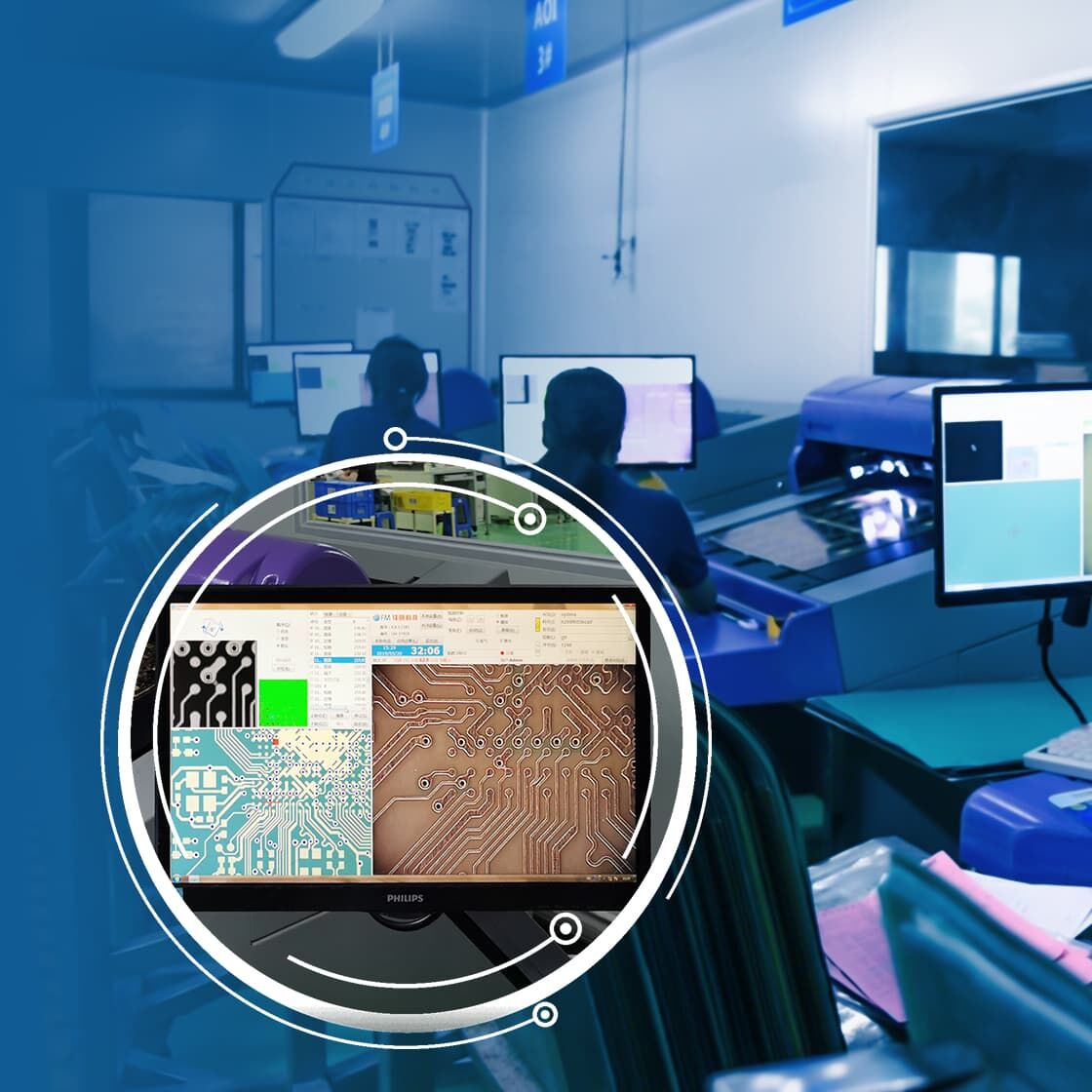
Aoi

Silkscreen
Aluminum PCB
Copper Based PCB