Quick Links

Home > PCB Manufacturing > Drills & Throughplating > Annular Rings
An annular ring refers to a donut-shaped metal pad on a PCB (printed circuit board) with a hole in the center for inserting component pins or wires. After soldering is completed, the annular ring establishes an electrical connection with the component pins inserted into its center hole, thereby achieving electrical connection between the various components on the PCB. The design and manufacturing quality of the "donut" is crucial to ensure the stability and reliability of the PCB electrical connection.
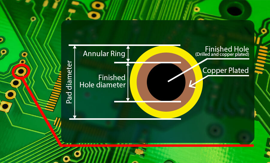
Generally speaking, the width of the annular ring is equal to half the difference between the pad diameter and the drill diameter. For example, if the drill diameter is 10 mil and the pad diameter is 24 mil, the width of the annular ring is:
(24 - 10) / 2 = 7 mil
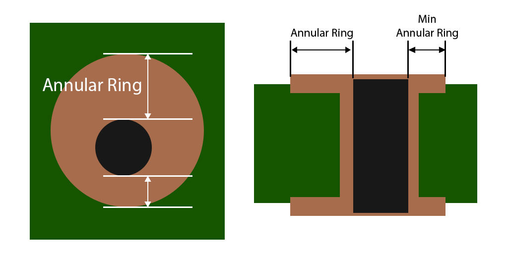
In order to make the electrical connection better, the width of the annular ring needs to be wide enough. During the design process, the minimum width of the annular ring should be greater than or equal to the minimum value specified by the design. If it is smaller than this size, it may affect the soldering connection of the components. In addition, it may also cause pad rupture (ie, the "zero annular ring" phenomenon), which means that the area where the circuit enters the pad is damaged, which will reduce the current carrying capacity of the circuit and even affect its normal operation.
Typically, the minimum width of the annular ring is 0.15mm (6 mil), and the drilling diameter range (CNC) is 0.2mm to 6.3mm. If it exceeds this range, the manufacturer may charge an additional fee. It is recommended to understand the relevant manufacturing tolerances before placing an order and reserve enough space when designing the PCB vias to ensure that the width of the annular ring is within an acceptable range to ensure the stability of the electrical connection.
During the manufacturing process of PCB, the drilling tool (drill bit) will be affected by various variables, resulting in the drilling position may not be completely located in the center of the pad, but there is a certain offset error, the following situations may occur:
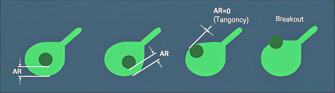
During the design and manufacturing process of PCB, undesirable situations such as tangency and rupture should be avoided as much as possible.
Plated Half-holes
PCBA Packaging
Conformal Coating
Surface Finish