Quick Links

Home > PCB Manufacturing > Printed Circuit Board > Heavy Copper PCB
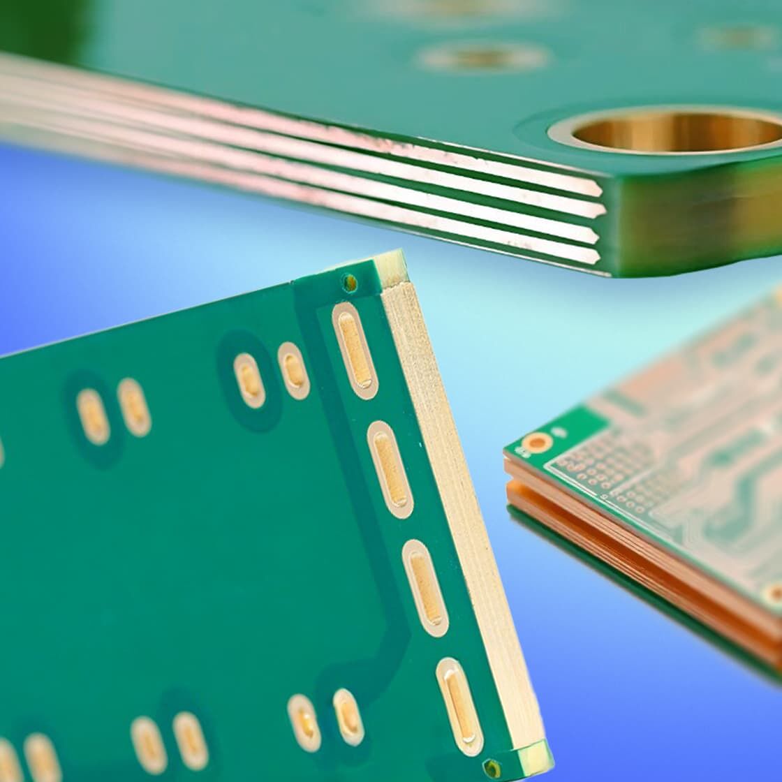
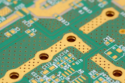
Heavy Copper PCB is a special type of printed circuit board. As its name implies, its core feature is that the thickness of the copper foil exceeds that of traditional PBC. The copper thickness of traditional PCB is usually between 0.5 and 2 ounces (i.e. 17.5 to 70 microns), while the thickness of Heavy Copper PCB is greater than 2 ounces. When the copper foil thickness reaches 10 ounces or more, this type of PCB is called Extreme Copper PCB, which is an advanced type of Heavy Copper PCB. In some extreme scenarios, the copper foil thickness can even reach 20 ounces (about 700μm), far exceeding the copper layer thickness standard of conventional Heavy Copper PCB.
As new energy, industrial automation and other fields develop towards high power and extreme environment adaptation, Heavy Copper PCB and extremely thick copper PCBs have become the key to meeting the needs of high current carrying and strong heat dissipation. The application scenarios of Heavy Copper PCB are also continuously expanding, including industrial control, new energy equipment, automotive electronics and medical equipment, and products with different copper thicknesses have different adaptation scenarios. Ultra-thick copper PCBs are adapted to more stringent conditions.
In order to comprehensively meet the requirements of electrical performance, mechanical strength and process adaptability, Heavy Copper PCBs usually choose insulating substrates based on high Tg FR-4 (Tg ≥ 150°C). In some scenarios, ceramic filling or metal-based composite materials or polyimide (PI) materials are used to enhance heat resistance, thermal conductivity and mechanical stress resistance, and adapt to the requirements of thick copper layer lamination and high-temperature operation.
In the context of increasingly stringent performance requirements for electronic products, Heavy Copper PCB has become a key choice to meet the requirements of electrical performance, heat dissipation performance, reliability, environmental adaptability, size and integration with its unmatched characteristics of ordinary copper thick circuit boards. Its significant advantages include:
The increase in copper foil thickness directly increases the conductor cross-sectional area, allowing Heavy Copper PCB to carry current and voltage far exceeding ordinary PCB. For example, equipment such as industrial power modules and electric truck power systems need to transmit large currents (often exceeding 5A). Ordinary copper wires (0.5-2 ounces) are prone to burn due to overheating, while Heavy Copper PCBs (especially above 4 ounces) can reduce resistance by increasing the thickness of the copper layer to avoid overcurrent risks; in high-voltage scenarios (such as power control systems), the physical structure of thick copper can better withstand electric field stress and reduce the risk of insulation breakdown.
Copper is an excellent thermal conductive material (thermal conductivity is about 401W/(m・K)), and the thick copper layer can be used as an efficient "heat dissipation channel" to significantly improve the heat dissipation efficiency. The heat generated by high-power devices during operation can be quickly diffused to the entire PCB through the thick copper pad, reducing the junction temperature of the device (compared with ordinary PCBs, the temperature rise can be reduced by 10-20℃); in a temperature cycle environment (such as -40℃~125℃), the thermal ductility of thick copper can relieve thermal stress, reduce line breakage caused by alternating hot and cold, and improve long-term operation stability.
The physical structure of Heavy Copper PCB gives it stronger damage resistance, especially for scenarios with strict reliability requirements. The increase in the thickness of the copper layer increases the mechanical strength of the routing and vias, can withstand vibration and impact (such as automobile engine compartments, rail transportation equipment), and reduce line breaks caused by mechanical stress; the bonding force between thick copper and the substrate is more stable, and copper foil peeling is not easy to occur in welding, rework and other processes, reducing the risk of functional defects.
Heavy Copper PCBs show stronger tolerance in harsh environments, far exceeding ordinary PCBs:
In the design of high-power equipment, Heavy Copper PCBs can carry large currents through a single wire, replacing the design of "multiple parallel wires" in ordinary PCBs, thereby reducing the number of PCB layers (such as from 8 layers to 6 layers), reducing the size of the board, and realizing equipment miniaturization. It also helps to reduce the number of components (such as reducing heat sinks and wire connectors) and optimize the overall system cost. Although the manufacturing cost of Heavy Copper PCB is higher, the full life cycle cost is lower.
Although Heavy Copper PCB has significant advantages in high current carrying and reliability, its unique material properties and manufacturing process also bring some unavoidable limitations. These shortcomings limit its applicability in specific scenarios, which are mainly reflected in the following three aspects:
The copper foil of Heavy Copper PCB is thick, and it is difficult to make thin and narrow lines during etching, so the line width and spacing need to be greater than 6mil; but the line width spacing required for high-density wiring is often less than 4mil, just like asking a "big guy" to flexibly walk in a "narrow alley", which is impossible. Therefore, Heavy Copper PCB can only be used in places such as power modules that do not pursue dense wiring, and cannot be competent for scenarios such as smartphone motherboards that require high-density signal transmission.
The production process of Heavy Copper PCB requires much higher process precision than ordinary PCB, and the core challenges are concentrated in:
In terms of materials, the amount of copper foil used is far more than that of ordinary PCB. In terms of processing, the complex etching and lamination processes extend the production cycle, and the scrap rate is high, further pushing up the processing costs.
In order to give full play to the advantages of Heavy Copper PCB, avoid manufacturing process difficulties and ensure performance, a series of targeted specifications should be followed when designing Heavy Copper PCB to balance function and manufacturability:
1. The minimum line width should not be less than 0.3mm to avoid line breakage due to etching difficulty;
2. The minimum spacing between adjacent traces should not be less than 0.25mm to prevent short circuit caused by incomplete etching;
3. The distance between the copper foil around the fixed hole and the hole edge should be ≥0.4mm, and there should be no thin wire within 1.5mm of the hole edge to enhance mechanical strength;
4. The distance between the trace and the edge of the PCB should be ≥3mm (it can be relaxed to 1.5mm in special cases, but the trace width should be ≥1.5mm at this time) to avoid edge stress causing copper foil to fall off;
5. The distance between high-frequency power devices and large capacitors should be 5mm to reduce signal interference;
6. The ground line width should not be less than 0.5mm, to ensure grounding reliability and heat dissipation efficiency;
7. The pad must not be directly connected to the bare copper foil or other pads to prevent welding short circuit;
8. It is necessary to design a dedicated heat dissipation structure for high-power components and adopt a low-density wiring solution to adapt to the thick copper process characteristics.
Feature |
Capability |
| Copper Thickness | 3 oz~12 oz(105 μm~420 μm) |
| Number of Layers | 4~12 layers |
| Substrate & Dielectric | FR4、CEM3 |
| Trace Width/Spacing | ≥4mil(0.1mm) |
| Mechanical Drilling | ≥1.0mm |
| Laser Drilling | ≥ 0.3mm |
| Lamination Temperature | 180~190℃ |
| Lamination Pressure | 300~400 PSI(2~2.8MPa) |
| Solder Mask Spacing | ≥ 3mil (0.075mm) |
| Screen Printing Spacing | ≥ 0.15mm |
| Surface Finish | HASL, OSP, ENIG |
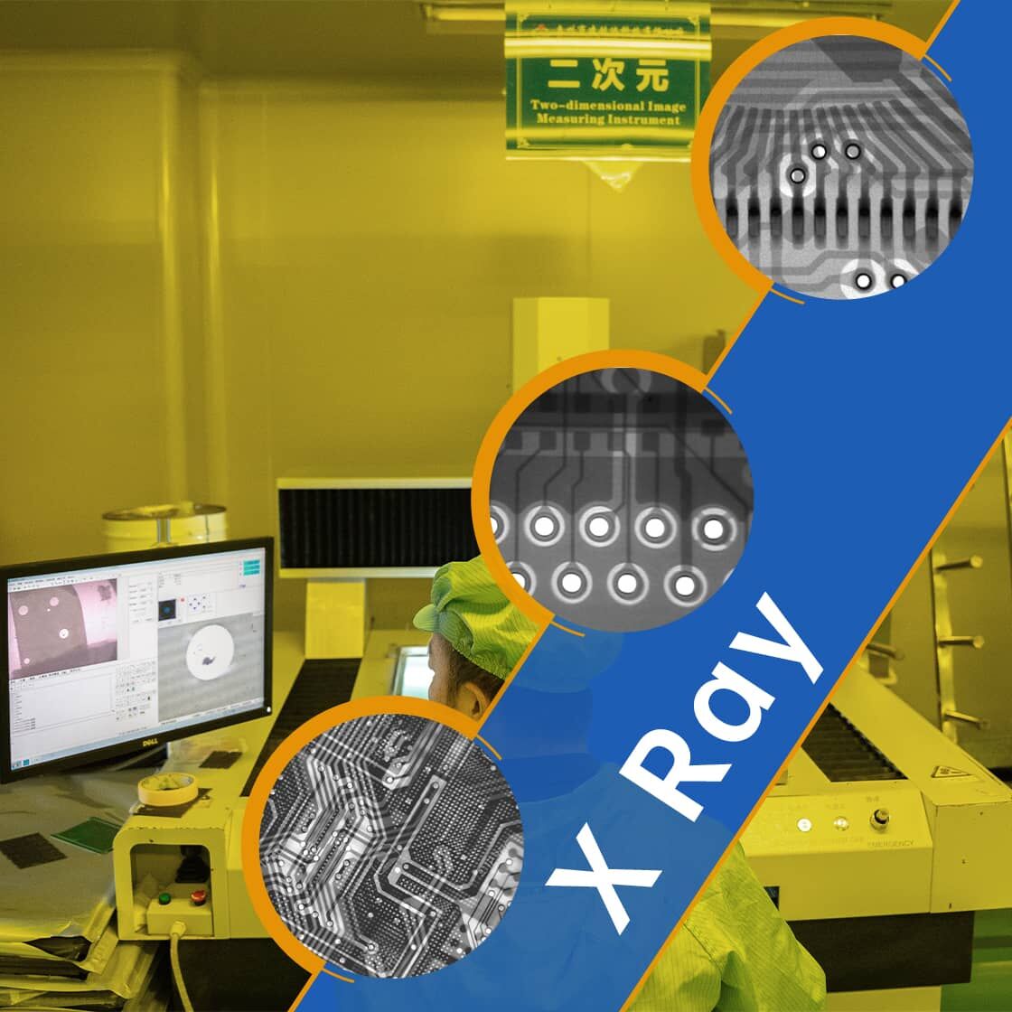
| Testing & Inspection |
AOI Electrical test X-ray inspection Thermal cycle test Mechanical strength |
| Special Process |
Hole filling Blue bar method Embedded Copper Thermal management design |
| Finished Product Packaging | Foam/Bubble Pad |
In the field of Heavy Copper PCB production, Linghangda has become the ideal choice for many customers with its profound heritage, excellent technical strength and all-round high-quality services. The following is a detailed explanation of the full reasons for choosing Linghangda:
If you are looking for a partner for the production of Heavy Copper PCBs, please feel free to contact Linghangda's sales team at any time, and we will immediately issue you a quotation plan.
Halogen Free PCB
HDI PCB
LED PCB
PCB X Ray