Quick Links
Home > PCB Manufacturing > Drills & Throughplating > Sideplating
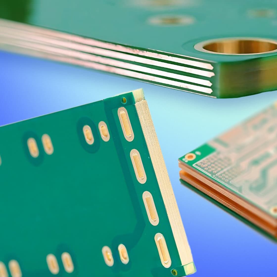
Side Plating, which we often talk about in the PCB industry, has a more vivid name called "edge copper plating", sometimes also called "Castellation". You can think of it as putting a layer of "copper coat" on the "side" of the circuit board - this layer of copper does not only cover the surface, but extends from the top layer of the PCB to the bottom layer, forming a complete conductive connection belt along the edge. This layer of copper is not simply covered on the edge surface, but is completely connected with the top and bottom conductive copper foils of the PCB itself, forming a conductive path that runs through the entire thickness of the board. Even in some designs, the edges of specific areas inside the board will also be metallized in this way, such as the edges of the grooves, cuts or separation areas reserved inside the PCB, which will also use the same metallization treatment method to make these internal edges conductive. This treatment can transform the edge of the PCB from an insulating frame that originally only serves as a physical support to a functional conductive structure that can participate in circuit connection.
After this layer of "copper coat" is completed, various surface treatments can be performed according to needs. For example, using the ENIG process, a thin layer of gold is covered on the copper layer to make the edge conductivity more stable and the oxidation resistance stronger; or using the ENEPIG process, a layer of palladium-nickel transition is added between gold and copper to further improve reliability; if you are pursuing cost-effectiveness, hot air leveling (HASL) is also a common choice. Covering the copper layer with molten solder not only protects the copper, but also facilitates subsequent welding.
In PCB design and manufacturing, side plating is not a general process, but a precise solution for specific functional requirements. Its advantages are particularly significant in the following scenarios:
For example, in RF modules, side copper plating can help reduce impedance and make high-frequency signal transmission more stable.
For example, the docking of sensor sub-board and motherboard, side copper plating can be directly used as "exposed contact", combined with the card slot design of the motherboard, the signal and power transmission can be completed without additional connectors, which simplifies the structure and saves space.
For PCBs that need to be frequently plugged in or may be subjected to lateral forces, side copper plating can enhance edge strength like a "metal skeleton". Its close combination with the substrate can reduce the risk of edge cracking and delamination, and is especially suitable for the durability improvement of thin PCBs (thickness ≤0.8mm).
In modular design, daughterboard needs to be connected to the motherboard quickly and stably. Side copper plating can replace traditional pin headers and achieve "plug and play" through edge welding or clamping. This design is not only more efficient in assembly, but also avoids poor contact caused by loose pin headers.
When the edge of the PCB needs to be welded and fixed (such as connecting to a metal housing or heat sink), side copper plating can provide a more reliable welding base. Its flat metal surface ensures uniform solder adhesion and avoids cold soldering or falling off, especially in automated welding, which can significantly improve the assembly yield.
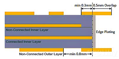
The effect of copper plating on the side depends largely on the control of details in the design stage. To ensure process feasibility and final quality, the metallization area must be clearly defined through "copper layer overlap" in CAD design, and the following core rules must be strictly followed:
This design can ensure the continuous coverage of the copper layer from the surface to the side during electroplating, avoiding "faults" - just like bricks need to be staggered and overlapped to be stable when building a wall, the overlap of the copper layer is the basic guarantee for the conductive performance of the side.
This part of the copper wire is equivalent to the "extension section of the wire", ensuring that the current can be smoothly transmitted from the inside of the PCB to the copper plating area on the side, avoiding excessive resistance or signal attenuation due to too narrow a connection.
This design is to prevent the copper layer in the non-functional area from being mistakenly connected to the side copper plating to avoid the risk of short circuit. At the same time, it reserves operating space for edge processing (such as cutting and grinding) to ensure that the accuracy of the side copper plating is not disturbed.
With its unique structure of "metallized edge", side plating shows irreplaceable value in improving PCB performance and reliability, especially in high-end electronic devices:
In high-frequency circuits, such as RF modules and 5G communication equipment, copper plating on the side can form an invisible barrier with the ground layer of the multi-layer PCB to block external electromagnetic interference (EMI) and reduce the external radiation of internal signals. This design can significantly reduce signal crosstalk and keep the circuit running stably in a complex electromagnetic environment.
For sensitive circuits, such as sensor modules of medical instruments, copper plating on the side can transform the edge of the PCB into a "shielding boundary" and form a full-range signal isolation space with the inner shielding design. This means that external stray signals are difficult to invade and internal key signals are not easy to leak, providing a pure working environment for high-precision circuits.
Electronic components are extremely sensitive to static electricity, and copper plating on the side can be used as an "electrostatic discharge channel" to guide the safe discharge of accumulated static charges during transportation and assembly, reducing the risk of electrostatic breakdown of components. This protective effect is particularly critical for bare boards without shell protection or modules that are frequently plugged in and out.
As the core carrier of edge connection, copper plating on the side can be used directly as a solder contact point, and can also be used in conjunction with the card slot to achieve mechanical fixation and electrical connection integration. This design not only simplifies the assembly process, but also improves the shock resistance and durability of the connection through the close combination of metal and metal, reducing failures caused by poor contact.
Although side copper plating can significantly improve PCB performance, it is limited by the characteristics of the manufacturing process. Potential risks need to be avoided in advance during the design stage to ensure process feasibility:
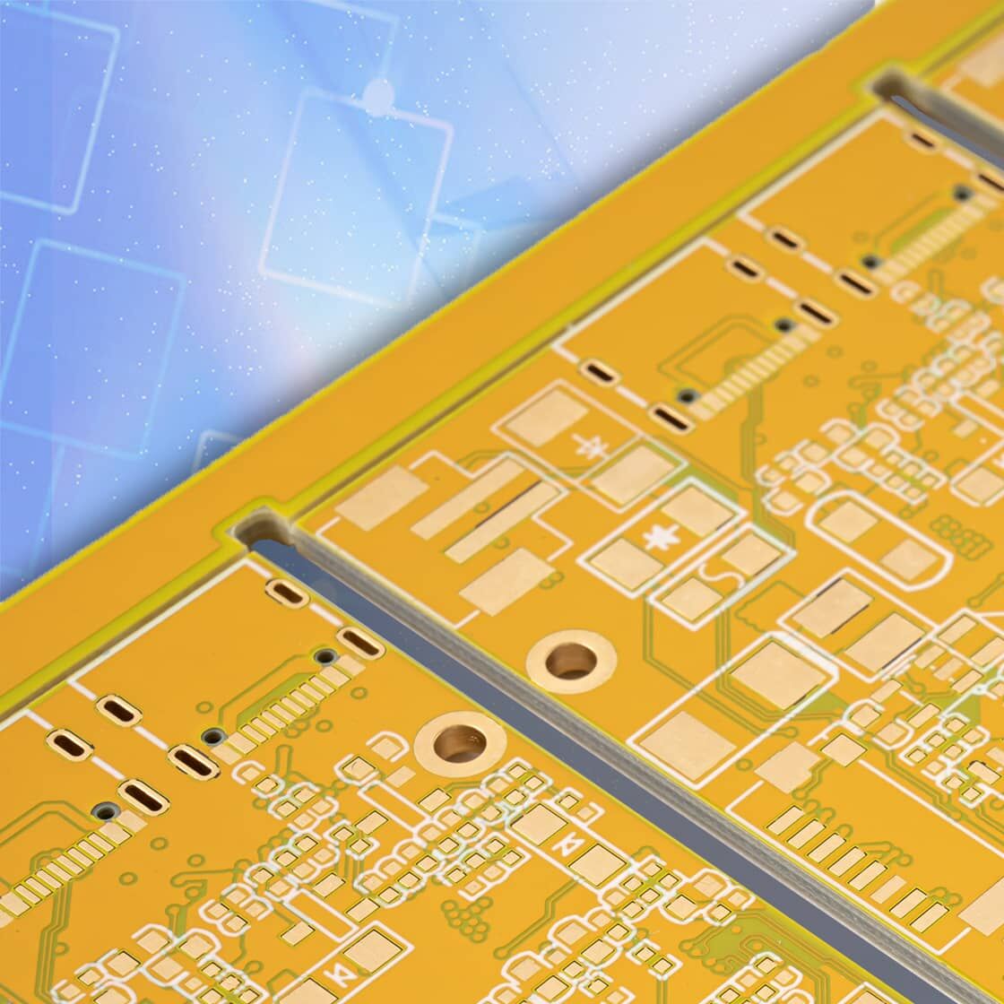
In PCB manufacturing, the board needs to be fixed on the production panel to ensure processing accuracy, which results in the side copper plating being unable to cover the entire length of the edge. This requires reserving a gap area at the corresponding position of the wiring label. This gap needs to be reserved according to the fixture design of the production panel, and the width is usually controlled at 2-5mm.
The metallization treatment of side copper plating needs to be completed before the through-hole electroplating (PTH) process, and V-Cut board separation will destroy the formed side copper layer, causing the plating to crack or fall off. Therefore, PCBs with side copper plating need to avoid V-Cut board separation. It is recommended to use the gong plate process to separate the boards and ensure the integrity of the edge plating.
The surface treatment of the copper-plated area on the side should give priority to immersion gold or immersion silver. These two processes can form a uniform and dense protective layer on the surface of the copper layer to avoid oxidation and do not affect the welding performance. If other treatment methods such as HASL are used, the reliability of edge connection may decrease due to uneven plating thickness.
At the same time, the solder mask design requires "solder mask opening" for the copper-plated area on the side to ensure that the metal surface is directly exposed to achieve conductive connection. To avoid ambiguity, it is recommended to add clear text notes in the design file to indicate the scope of the copper plating on the side, the type of surface treatment and the connection requirements, so that we can execute it accurately.
Copper Based PCB
Heavy Copper PCB
Plated-through Slots
PCB Testing