Quick Links

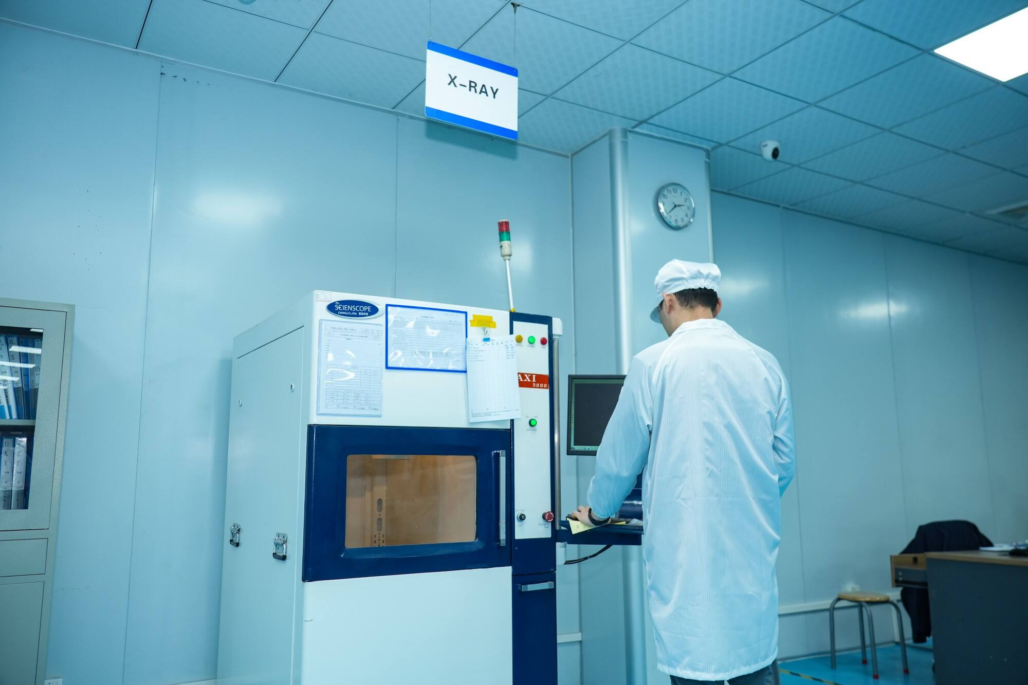
Automated X-ray Inspection (AXI) is an automated inspection technology that uses X-rays as an observation tool. It shares the same operating principle as Automated Optical Inspection (AOI), but instead of relying on visible light, it leverages the strong penetrating properties of X-rays to see deep into objects. If AOI is like using the eye to see the surface, AXI is like installing a X-ray machine on the PCBA. X-rays can easily penetrate materials impermeable to visible light, such as component packaging and PCB substrates. By capturing the differences in X-ray absorption across different materials, they produce clear images of internal structures, enabling precise identification of underlying issues such as dimensional deviations, positional offsets, and hidden defects.
This comprehensive inspection capability is crucial in PCBA manufacturing. It uncovers hidden dangers, such as voided solder joints and loose pin connections, hidden beneath the packaging and within multilayer boards. It becomes an indispensable eye for quality control.
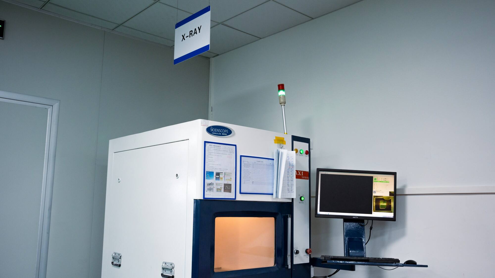
As electronics manufacturing evolves towards higher density and miniaturization, array-based packaged devices such as BGAs, QFNs, CSPs, and flip chips have become mainstream. The solder joints of these devices are hidden on the underside of the package, making traditional inspection equipment like AOI ineffective due to their inability to penetrate light. Furthermore, the continued shrinking of component packages and increasing PCB wiring density highlight the irreplaceable role of AXI: X-rays can easily penetrate the package casing, directly reaching the solder joint area, and accurately inspect the quality of hidden solder joints, thus preventing circuit failures caused by solder joint problems at the root.
Leveraging X-ray's penetrating imaging capabilities, AXI can accurately capture a variety of PCBA assembly defects, including but not limited to the following:
1. Solder joint quality issues: such as insufficient solder, cold solder joints, bridging, and bubbles;
2. Hidden defects: In high-density layouts, defects such as pin offset and pad misalignment are difficult to detect with the naked eye;
3. Structural anomalies: Different materials absorb X-rays differently. The higher the density of the material, the stronger the absorption, resulting in clearer image shadows. These differences can be used to identify problems such as delamination and foreign material inclusions within the PCB.
These inspections not only detect defects but also trace their root causes through image analysis, providing data support for process optimization.
AXI technology has evolved from traditional 2D imaging to 3D inspection:
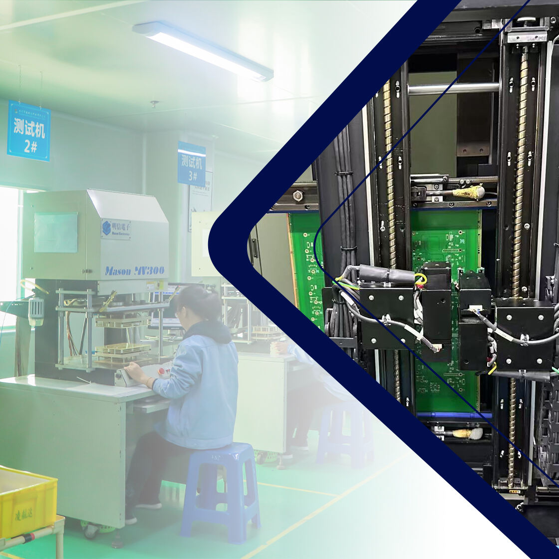
In PCBA manufacturing, AXI is the "last line of defense" for ensuring product reliability. PCBally promises that all PCBA products leaving the factory undergo thorough AXI inspection. Whether it's solder joints hidden under the BGA or subtle defects in high-density layouts, they are accurately identified and corrected, ensuring that every product meets design standards and application requirements.
IC Programming
Solder Mask
HDI PCB
PCB Testing