Quick Links

PCB X-ray inspection is a nondestructive testing method that uses X-ray technology to examine the internal structure of printed circuit boards (PCBs). This advanced technology allows manufacturers to view the interior of complex PCBs without destroying the board, revealing hidden defects that are invisible to the naked eye but could cause product failure.
While traditional optical and visual inspections remain valuable, they only provide surface-level inspections. PCB X-ray inspection takes quality control to a new level, offering the following advantages:
• Internal Visibility: X-rays can penetrate the multi-layer structure of a PCB, revealing issues within the board.
• Higher Accuracy: X-ray systems can detect tiny defects invisible to the naked eye.
• Comprehensive Analysis: From solder joint integrity to component positioning, X-ray inspection covers a wide range of potential issues.
As PCB designs become increasingly complex, X-ray inspection is becoming increasingly important, particularly for:
• High-density interconnect (HDI) boards
• Multi-layer PCBs
• Boards containing ball grid array (BGA) components
• Miniaturized electronic products with complex internal structures
These advanced PCBs often contain hidden solder joints, inner-layer vias, and high-density components that are difficult to inspect visually, making X-ray technology an indispensable quality assurance tool.
PCB X-ray inspection is based on the same physical principles as medical X-rays. The process is as follows:
1. X-ray emission: A controlled X-ray beam is emitted toward the PCB.
2. Penetration: The X-rays pass through the PCB's multilayer structure and components.
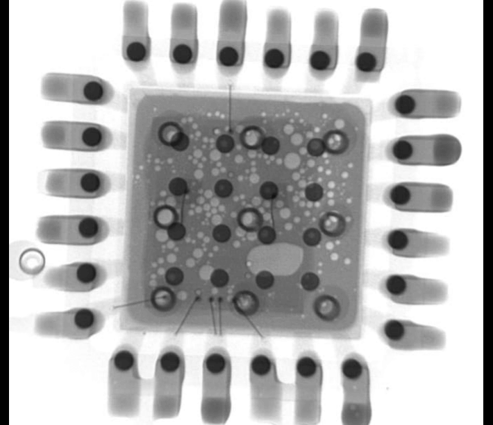
3. Absorption: Different materials absorb X-rays to varying degrees, creating contrast.
4. Imaging: A detector on the other side of the PCB receives the signal after penetration.
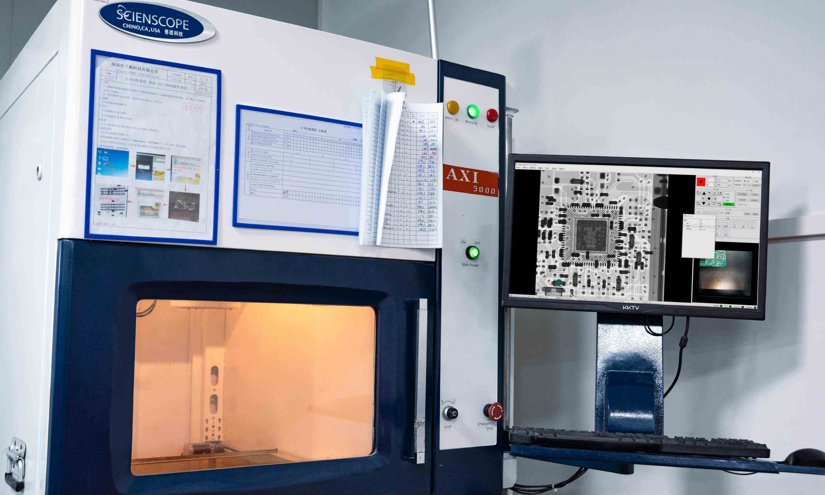
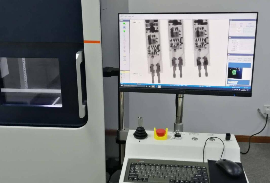
1. Sample Preparation: The PCB is placed in the X-ray equipment, typically on a movable table for precise positioning.
2. Parameter Setup: A technician adjusts the voltage, current, and exposure time to optimize image quality.
3. Scanning: The X-ray beam scans the PCB at different angles to capture images.
4. Image Processing: Advanced software enhances the raw X-ray image for improved clarity and analytical accuracy.
5. Inspection: A trained operator or AI system analyzes the image to identify defects or anomalies.
6. Reporting: The inspection results are generated, along with an image highlighting any problem areas.
o Provides a planar top-down view of the PCB
o Suitable for quick inspection and detection of obvious defects such as solder bridges
o Limited depth information, making it difficult to identify delamination defects
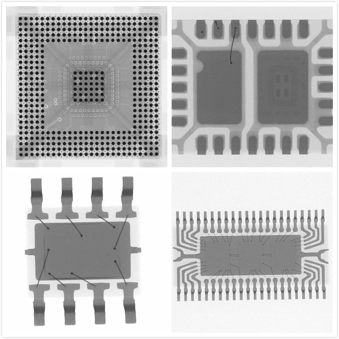
o Combines multiple 2D images taken at different angles
o Provides a sense of depth, revealing hidden solder joints
o Better suited for inspecting complex components such as BGAs
o Creates a complete three-dimensional model of the PCB's internal structure
o Allows for "virtual slicing" without damaging the board
o Provides the most comprehensive inspection, but is time-consuming and costly
Although aluminum-based PCBs have many advantages, they still have some disadvantages:
o Resolution and Magnification
o 2D, 2.5D, or 3D CT Capabilities
o Ability to Process the Required Size and Type of PCBs
o Years of Industry Experience
o Familiarity with the Type of PCBs You Produce
o Technician Qualifications and Certifications
o Ability to Meet Production Schedules
o Ability to Handle Volume Orders
o Level of Detail and Clarity of Inspection Reports
o Interoperability with Your Quality Management System
o Actionable Improvement Recommendations
o Responsiveness
o Willingness to Collaborate on Problem Solving
o Flexibility to Address Special Needs
PCB X-ray inspection has become a vital tool in the pursuit of perfection in electronics manufacturing. It provides insight into the hidden layers of a PCB, revealing potential defects and quality issues—a crucial role in ensuring the reliability of everything from medical devices to the performance of smartphones.By adopting this technology, manufacturers can:
• Detect and resolve issues early in production
• Improve overall product quality and reliability
• Reduce costs associated with failures and recalls
• Stay ahead in a competitive market
As PCB designs become increasingly complex and miniaturized, the importance of X-ray inspection will only grow. Forward-thinking companies are incorporating it into their quality management processes, resulting in higher yields, greater reliability, and increased customer trust.
Don't let hidden defects compromise your product quality. Partner with PCBally and leverage our advanced X-ray inspection technology to ensure your PCBs meet the highest quality standards. Contact us today to learn how we can support your commitment to excellence in electronics manufacturing.
Through-Hole Assembly
Solder Mask
Teflon PCB
PCB Packaging