Quick Links
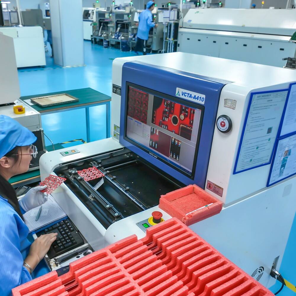
E-Test, short for electronic testing, is used to inspect circuit boards for shorts, opens (compared to the netlist), resistance, and capacitance. After testing, a series of reports are generated based on the results, including cross-sectional analysis, peel strength, and solderability. This ensures that the bare board will function and perform optimally in the actual application.
As PCB designs become increasingly complex, with smaller feature sizes, higher routing density, and ever-shrinking drill holes, electronic testing has become crucial for PCB quality control. Visual inspection, previously the primary method, is no longer sufficient, as it was only suitable for inspecting two-layer or multi-layer PCBs prior to lamination. Furthermore, with the advancement of through-hole technologies like blind and buried vias, visual inspection has become difficult to achieve the required inspection depth.
Some people believe that as long as there are no errors during PCB manufacturing, electronic testing is no longer necessary. This is a common misconception. Each step in the production of a PCB is a separate process. Therefore, each PCB must be tested. Only electronic testing can identify incorrect or missing connections. Only after passing electronic testing can a PCB be fully functional. Electronic testing is a critical process to ensure that there are no shorts or opens before PCBs are delivered to customers or assembled into devices.
During testing, PCB manufacturers primarily check for two types of defects: opens and shorts. Other types of testing can be performed based on customer needs. There are two main types of electronic testing:
This method requires the use of a PCB fixture test device. Its disadvantage is that a dedicated test fixture is required for each PCB, making it unsuitable for prototype boards. However, with flexible probes, the fixture can simultaneously contact all points requiring electrical testing, typically taking 5 to 10 seconds to test a single PCB. This testing method can significantly improve production efficiency and is suitable for mass production.
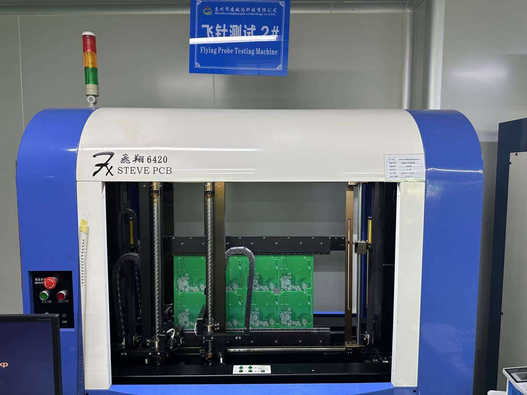
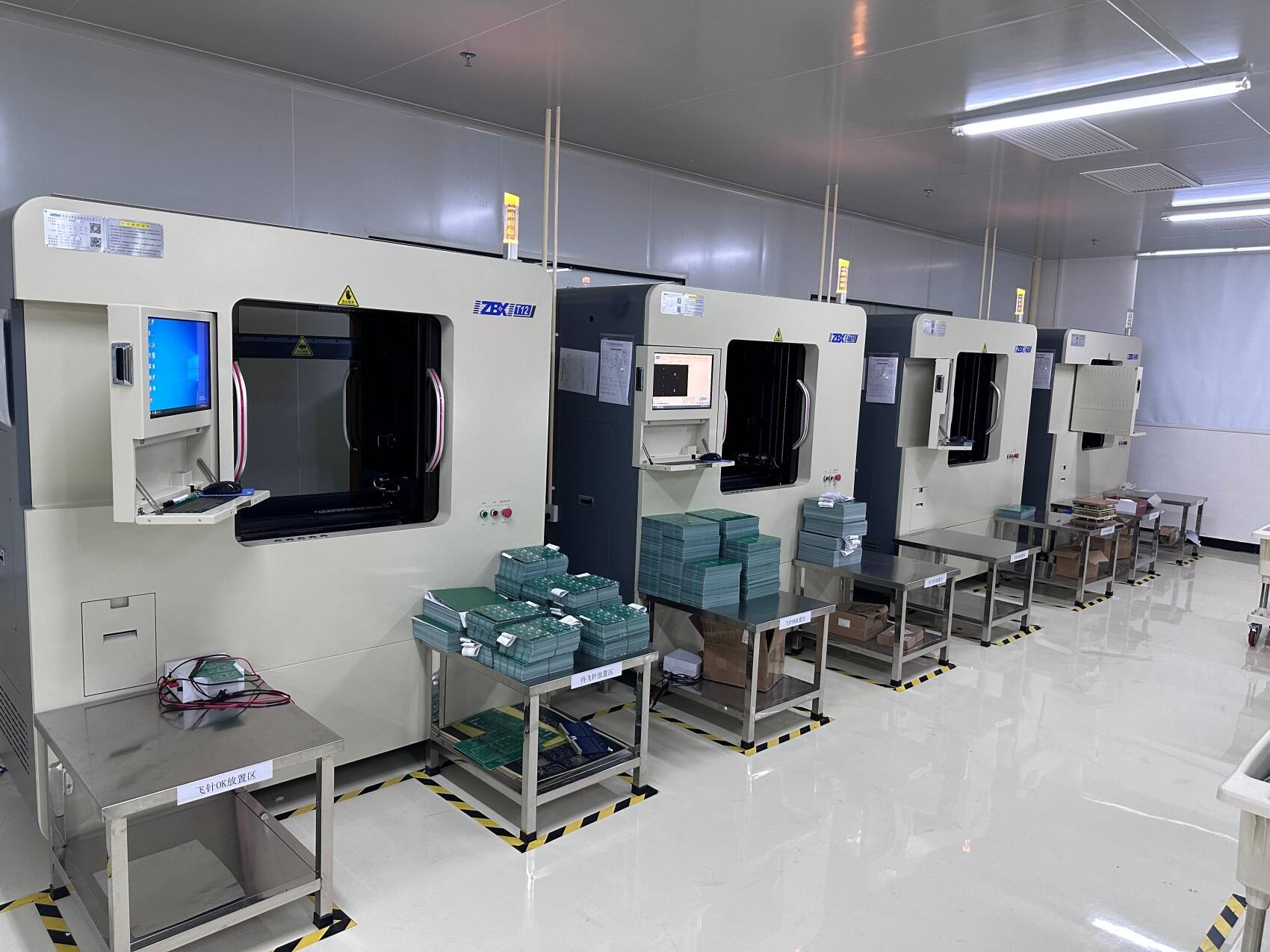
This method uses a flying probe tester to inspect each PCB's connected networks one by one. Programmable test probes can directly contact pre-set measurement points such as wires, pads, pins, and test points to check for connection errors. This process eliminates the need for test fixtures, significantly reducing customer costs. Typically, the test time per PCB is 1-3 minutes. Flying probe testing is suitable for prototype boards and small batches of bare board products. Each network can be checked using a flying probe tester to ensure its integrity and that it is not short-circuited with other networks. Flying probe testing offers the advantages of low cost, short lead times, and the absence of fixed test tools.
PCBally is committed to providing high-quality PCB manufacturing services that meet our customers' needs and expectations. 100% of our PCBs undergo electronic testing at the end of the production process, ensuring they are 100% ready for use when delivered to you. If you have additional testing requirements, please contact us via email or online customer service.
Plated-through Slots
Surface Finish
Box Build Assembly
A.O.I.