Quick Links
Home > PCB Manufacturing > Printed Circuit Board > Gold Finger PCB
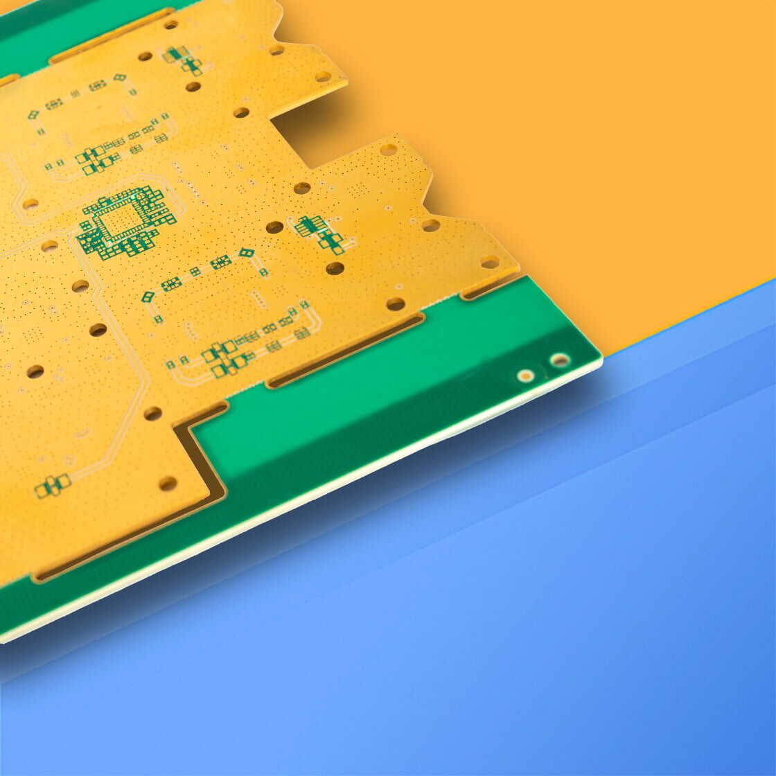
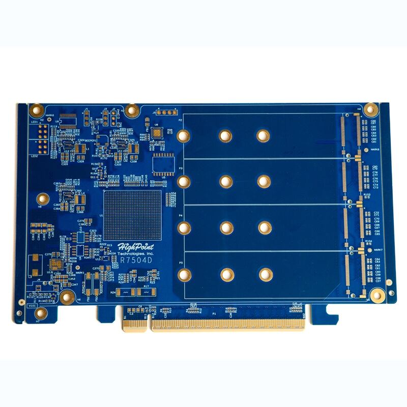
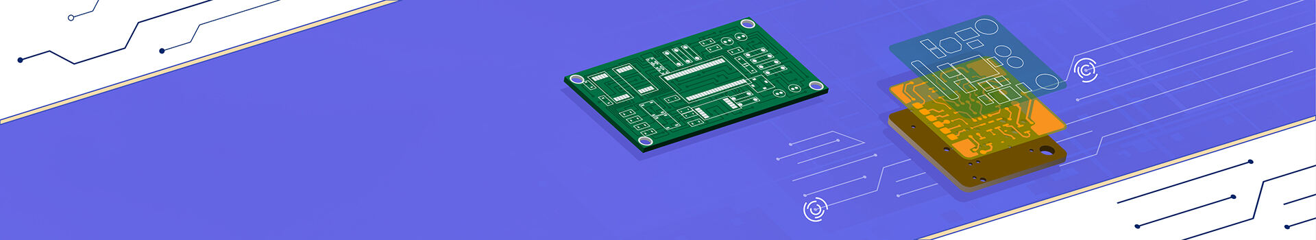
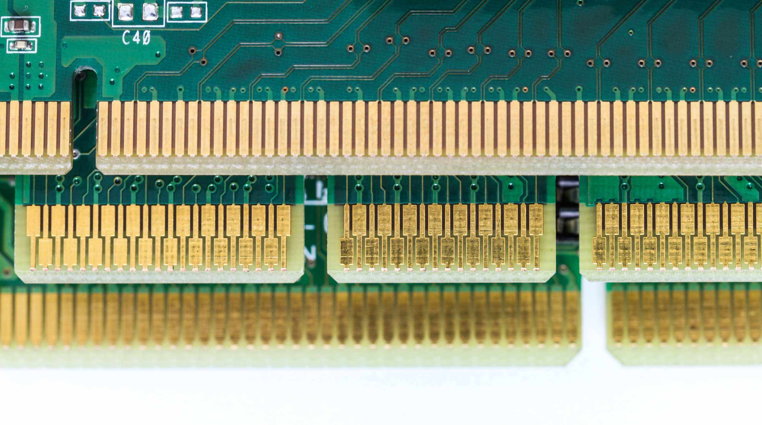
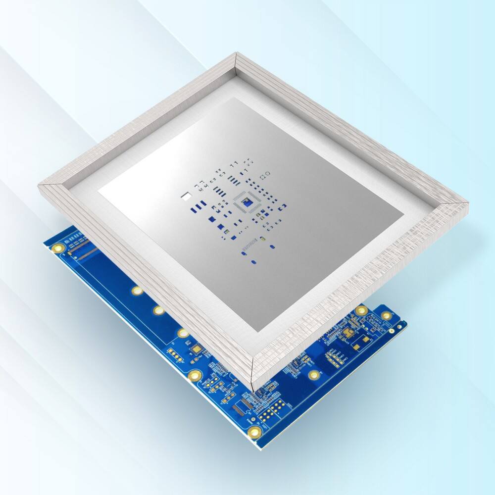
Simply put, a gold finger PCB is a row of golden contact points (pads) specially made on one or more sides of the board. These pads are very precious: they are deliberately not covered with green oil (solder mask), and a thick layer of hard gold (usually 10 to 100 micro inches thick) is electroplated on the surface. Because these gold-plated pads are of the same size, neatly arranged, and in the same direction, they look like rows of golden fingers from a distance, so everyone calls it "gold fingers".
Think about the USB flash drives and memory sticks in computers that are plugged in and out every day. These devices have extremely high requirements for the wear resistance and reliability of the interface. Gold has two natural advantages. One is that it has strong corrosion resistance and is not easy to oxidize and rust, ensuring long-term stability of the contact points. The second is that gold has excellent conductivity, smoother signal transmission and less loss.
Therefore, although the cost of gold plating is much higher than the common chemical immersion gold (ENIG) process, gold fingers are the best solution in situations where frequent plugging and unplugging is required or the signal quality is demanding, and they play an important role in the electronics industry.
Like us, Linghangda has been rooted in the industry for more than 20 years. The team, from engineers to front-line technicians and customer service, are all experienced "veterans". We are well aware of the essence of gold finger technology and control quality throughout:
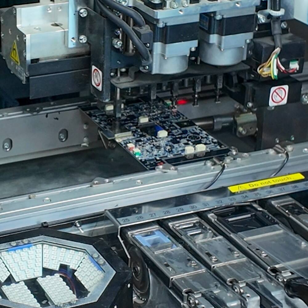
From the entry of raw materials to the shipment of finished products, the entire process strictly follows the ISO9001 quality management system, and every link is tightly controlled.
With strong supply chain integration capabilities and lean production management, we can not only guarantee the high quality of gold finger PCB (especially the thickness and uniformity of gold plating), but also provide competitive prices.
The highly professional sales team follows up throughout the process, from your inquiry, order, follow-up to delivery and after-sales, with quick response and smooth communication.
Our product consumption covers more than 150 countries, which is the best endorsement of our product quality and professional service. Choosing us means choosing a reliable one.
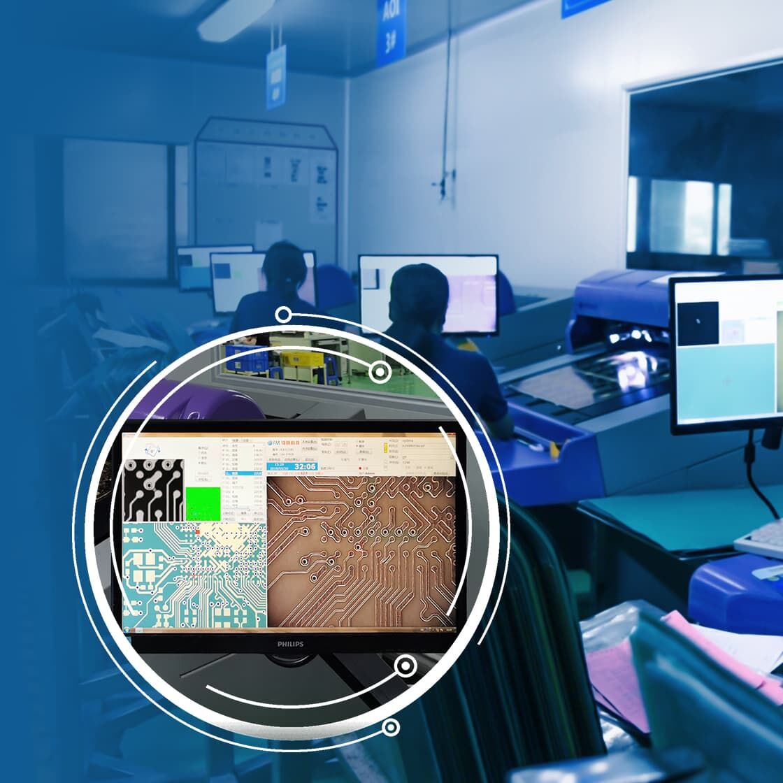
1 piece to 100,000 pieces, same price and same quality. No minimum order quantity, even if you only make 1 piece, you can enjoy the bulk price. The whole process follows ISO9001 and UL certification standards, and each batch of shipments can provide 100% electrical testing, AOI inspection and X-Ray reports, the quality is clear at a glance.
Gold fingers are also divided into different types according to design requirements:
The most common, a row of uniform rectangular gold "fingers" on the edge of the board, with the same length and width.
The pads are also rectangular, but when arranged on the edge of the board, the length will change in segments, which looks "disconnected", and is often used in designs with specific timing or power requirements.
The pads are still rectangular, but the length of each gold finger is different, specially designed to optimize specific performance.
This is not for appearance, the core purpose is to achieve better performance and more stable connection:
Plating a uniform and thick hard gold on the gold finger is a key process. There are two mainstream electroplating methods:
Make auxiliary wires next to the gold finger to conduct gold plating. After plating, use a milling cutter to cut the edges or etch away these wires. The problem with this method is that a little copper may remain on the edge of the gold finger after processing, which violates the high standard requirement of "the area around the gold finger must be clean and no copper should be exposed".
Smartly use the existing circuit routing on the inner or outer layer of the PCB board to cleverly lead the current to the area that needs to be gold plated. In this way, there is no need to make additional leads next to the gold finger, and the risk of copper exposure on the edge is completely eliminated. Of course, this requires internal space wiring of the board. If the circuit density is too high and there is no "road" inside, this method is more difficult to implement.
Gold finger electroplating is a delicate job, and it is inevitable to encounter some minor problems. We have accumulated a lot of practical experience to deal with it:
The most common problem is the problem of gold plating solution - low gold concentration, wrong ratio, uneven stirring, or contamination by metal impurities such as nickel and copper. Solution: Add gold salt when necessary, adjust the solution ratio, strengthen stirring, and most importantly, remove the metal impurities in the gold solution.
It may be that the copper and nickel are not tightly attached, or the nickel and gold are not firmly attached. It may also be that the board surface was not cleaned before nickel plating or the nickel layer itself was too tight due to excessive stress. Solution: Focus on optimizing the cleaning and activation process of the copper and nickel surfaces, and strengthen pretreatment; at the same time, purify the electroplating solution, "clean up" the nickel tank or treat it with activated carbon.
It is often because the additives in the gold plating solution are insufficient, the pH value of the solution is high, or it is contaminated by metal ions such as nickel ions. Solution: Add additives in appropriate amounts, adjust the pH value back to normal, and work hard to remove the metal ions that contaminate the gold solution. Daily protection against nickel ion pollution is the key!
Mostly, the cleaning after electroplating is not clean, the medicine is residual, or the storage environment is not good, and there are corrosive gases. Solution: Be sure to thoroughly clean and dry after gold plating! The finished board should also be placed in a dry and clean environment.
Gold itself is not easy to oxidize, but if it is exposed to the air for a long time, a very thin oxide film may form on the surface or absorb dust and oil, resulting in increased contact resistance and poor contact. Don't worry, it can be restored with simple treatment:
Feature |
Capability |
| Gold Finger Finish | Hard gold plating (Au) thickness commonly 3-5 µm |
| Gold Finger Thickness | Common gold plating thickness: 3 µm (min.) |
| Chamfer Angle | Typically 30° to 45° chamfer angle |
| Chamfer Depth | Around 0.2 to 0.5 mm |
| PCB Thickness | Usually 1.0 to 1.6 mm |
| Solder Mask Opening | Defined clearance from gold finger edge |
| Copper Thickness | Base copper thickness around 1 oz/ft² (35 μm) |
| Edge Connector Length | Length of gold finger area varies by design |
| Surface Roughness (Ra) | Controlled to ensure good gold adhesion |
| Gold Finger Width & Spacing | Based on IPC standards (commonly ~0.5 mm width) |
In the final analysis, the core function of the gold finger is to build a bridge - to reliably connect the PCB with other electronic components and complete equipment to establish a stable electrical channel. It is an indispensable connection port in various devices such as computers, mobile phones, game consoles, printers, smart home appliances, etc. That layer of hard gold is the "golden armor" that resists oxidation corrosion and ensures high-speed and stable signal transmission. Therefore, the gold finger wiring technology is the key to achieving efficient, reliable and durable connections between devices. It has outstanding cost-effectiveness and is a widely trusted solution in modern electronic manufacturing (especially OEM). Only by selecting and doing this "golden signboard" well can the equipment run stably and efficiently.
Smt Assembly
Aoi
PCB Stencil
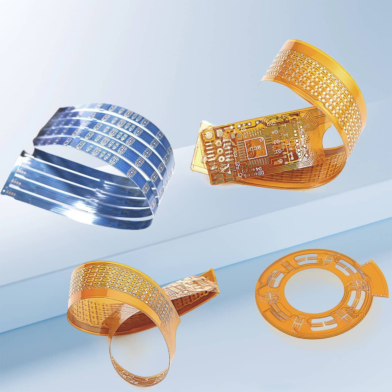
Flexible PCB