Quick Links

Home > PCB Manufacturing > Printed Circuit Board > High Frequency PCB
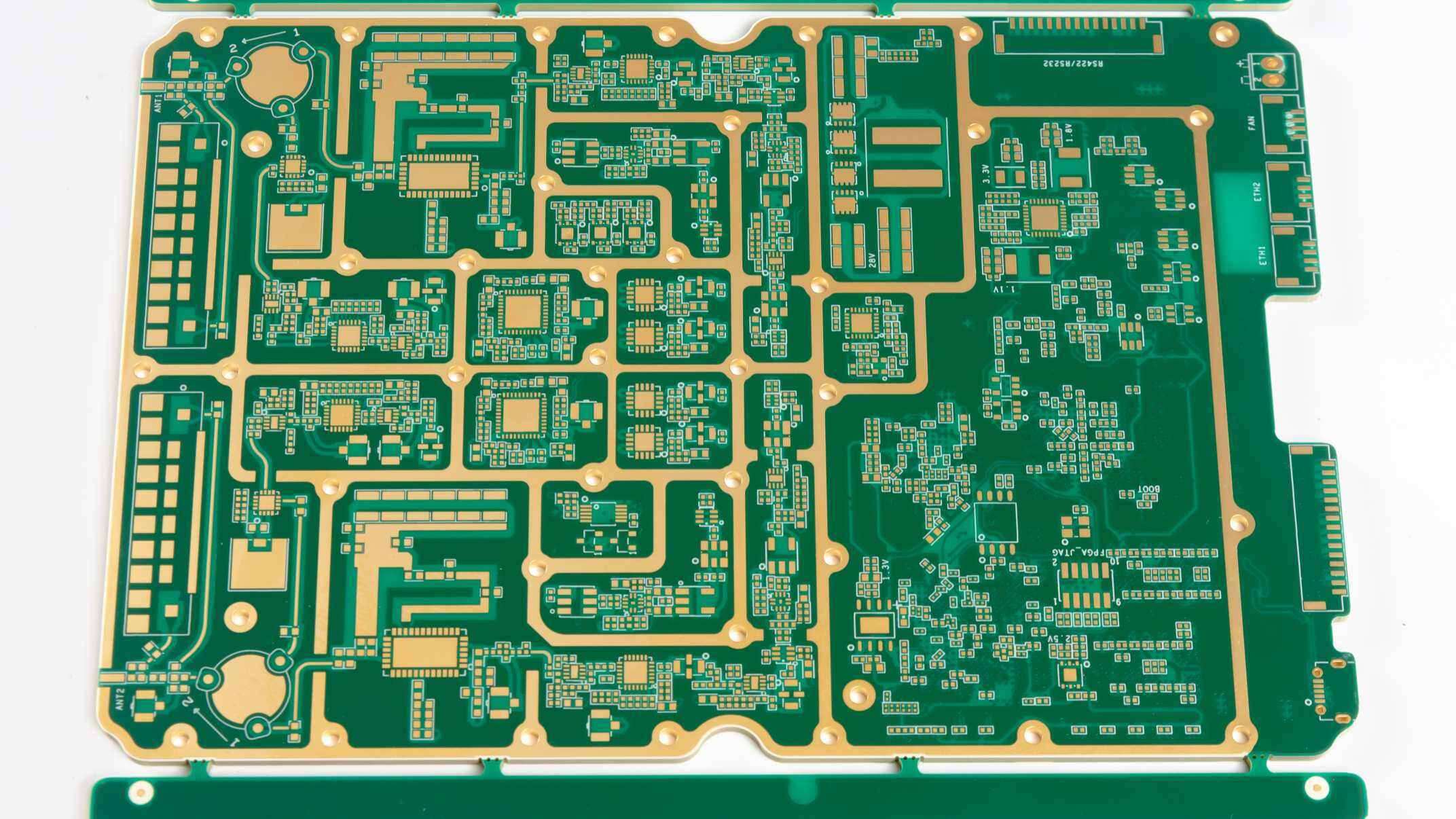
A high frequency circuit board is a printed circuit board designed to transmit signals above 1GHz. It minimizes signal loss, distortion or reflection. These RF circuit boards use copper-clad materials (such as RO4350B, RO3010 and PTFE) with low dielectric constant (Dk) and low dielectric loss (Df). This maintains impedance accuracy and reduces insertion loss in the GHz band.
High-frequency PCBs strictly control parameters such as dielectric thickness, copper foil roughness and trace width. The purpose is to achieve stable impedance and prevent signal degradation. It is different from standard FR4 circuit boards. High-frequency circuit designs use temperature-stable and frequency-stable materials. This reduces phase delay and signal dispersion.
High-frequency PCB manufacturers mainly produce these boards for RF and microwave systems. They are used in radars, antennas, satellite receivers, and millimeter-wave circuits, etc. These fields have high requirements for signal integrity and frequency performance.
Low Df copper clad laminate materials, such as RO3003 and RO4350B, are commonly used in high-frequency PCBs. They effectively reduce insertion loss at microwave and millimeter-wave frequencies.
Stable dielectric thickness and trace width can control impedance to within ±10%. This ensures the waveform integrity of high-speed RF circuits.
The moisture absorption rate of high-frequency copper clad laminates is usually less than 0.02%.
Blind vias, buried vias and back drilling technologies are used. This shortens the residual length of vias and improves the return loss of high-speed signal layers.
Reasonably arrange ground vias, solid reference layers and trace spacing. This effectively controls radiated emissions and reduces crosstalk between signals.
High-frequency substrates have good thermal stability. Under reflow soldering or continuous high temperatures, it can prevent delamination and copper foil shedding.
Rogers RO4350B, RO3003, and RO3010 offer stable dielectric constants (Dk between 3.0 and 10.2). They have extremely low dielectric losses (0.0013 minimum). They are suitable for antenna feed networks and broadband filters, etc. These materials support frequencies up to 77GHz. They are widely used in RF front-end circuits, phased arrays, and power amplifiers, etc.
Taconic materials have good thermal stability and extremely low moisture absorption. They are very suitable for high-frequency signal paths. TLX materials have low insertion loss and excellent thermal stability. They are suitable for multi-GHz power amplifiers and RF switching circuits. They are compatible with standard PCB manufacturing processes.
Arlon 85N has high thermal conductivity (0.20 W/m·K) and good copper foil adhesion. Its glass transition temperature is as high as 250°C. It is an ideal choice for high-power radar transmitters and extreme environment RF modules. Suitable for high-power RF circuits and high-frequency PCB applications in harsh working conditions.
Isola's E-glass fiber reinforced materials are cost-effective and have good signal performance below 10GHz. They are a mid-range solution between traditional FR4 and PTFE systems. Suitable for applications below 5GHz.
Feature |
Capability |
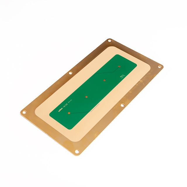
| Substrate Materials |
Isola Nelco Taconic PTFE Ceramic-filled PTFE Rogers RO4003C/RO4350B |
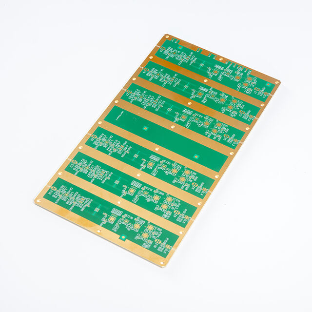
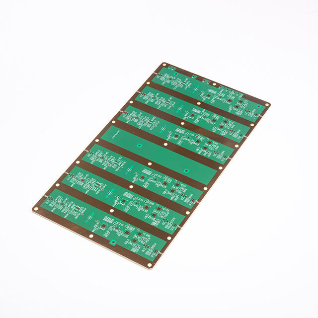
| Layer Count | 2~20 layers |
| Solder Mask Spacing | ≥ 3 mil (0.075 mm) |
| Solder Mask Color | Green, White, Black, Red |
| Copper Thickness | 0.5~2 oz(17.5~70 μm) |
| Minimum Line Width/Line Spacing | 2~5 mil(0.05~0.127 mm) |
| Minimum Mechanical Aperture | 0.15~0.2 mm |
| Minimum Laser Micro-Aperture | 0.1 mm |
| Dimensional Tolerance |
±0.1 mm (board thickness) ±0.05 mm (outline) |
| Special Processes |
Plasma/chemical roughening Low loss solder mask Micropore filling Layer lamination Strict board baking |
| Frequency Range | ≥1~60 GHz |
| Dk | 2.2~3.8 GHz |
| Df | ≤0.005 GHz |
| Tg | 280℃ |
| Td | ≥390℃ |
| CTE | 32~60 ppm/℃ |
| Thermal Conductivity | 0.6~0.8 W/m·K |
| Water Absorption | ≤0.1% |
| Finished Product Packaging | Foam/Bubble Pad |
Widely used in 5G base stations, microwave backhaul links and satellite ground systems. Applied in antennas, RF amplifiers and filters.
MRI, CT and diagnostic imaging systems rely on compact, low-noise RF PCB designs. This ensures stable high-frequency signal transmission.
High-frequency circuit boards support radar modules operating at 24GHz and 77GHz. Used in adaptive cruise control and collision warning systems.
Used in avionics, navigation systems and safety communications. Applied in radar arrays, telemetry systems and satellite communication modules (SATCOM).
Enable Wi-Fi, GPS and Bluetooth functions in smartphones, tablets and IoT devices.
Upload Gerber files or create board layouts with our online PCB design tool. Make sure the files are complete and in the correct format. This ensures smooth subsequent processing.
Customize your order according to your needs. Including number of layers, size, thickness, copper foil weight, solder mask color, surface treatment, etc. Our system interface is simple and intuitive, and easy to configure.
Once the design and specifications are confirmed, the system displays the price in real time. You can adjust the configuration options according to your budget.
Check the documents and specifications for correctness, enter the secure checkout process, and select the payment method. You will receive a confirmation email and order details after the order is successfully placed.
Your circuit board will be put into production immediately. We will provide progress updates throughout the manufacturing process. After completion, it will be properly packaged and delivered to your address in a traceable manner.
Through-Hole Assembly
First Article Inspection
A.O.I.
Halogen Free PCB