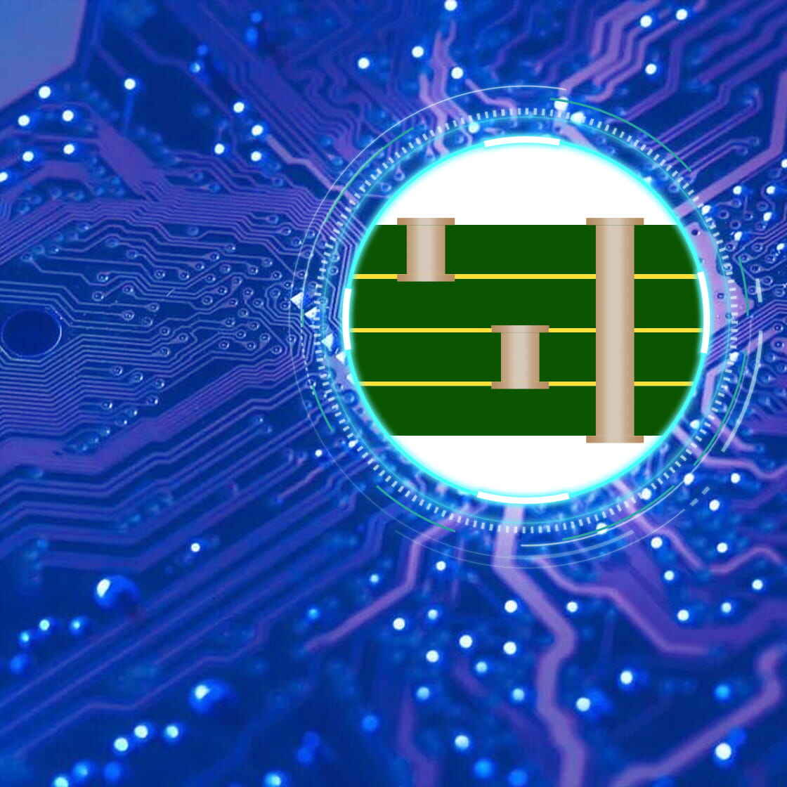
What are plated half-holes?
Plated half-holes, also called castellated holes, are holes that are only half the shape of a through hole. They are mainly used to solder small circuit board modules to large circuit boards, such as installing Bluetooth modules or Wi-Fi modules on the main circuit board. Plated half-holes are a common connection method.
How to design a plated half hole?
When designing a plated half hole, pay attention to the following points:
-
Place the center point of each plated half hole on the edge of the PCB (if it is an elliptical hole, pay attention to the start and end positions). In the design software, define these holes as plated through holes.
-
If you use a Gerber file, make sure these holes or slots are in the drill file, such as the file name may be .drills_pth.xln or .pth.drl.
-
Each plated half hole must have a pad on each copper layer (including the inner layer of a four-layer board) to ensure the stability of the copper sleeve.
-
The pad must completely surround the hole, and the design requirements are the same as ordinary through holes.
-
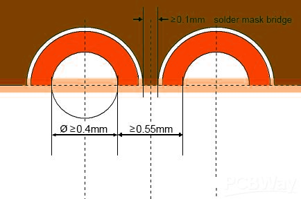
The minimum half hole diameter is generally 0.6mm, but PCBWay can accept a minimum diameter of 0.4mm.
-
The minimum edge spacing between holes is 0.55mm; if the spacing is between 0.47mm and 0.55mm, the manufacturing cost and time will increase.
- The minimum width of the solder mask bridge is 0.1mm.
Manufacturing process of electroplated half-hole
The traditional manufacturing process of electroplated half-hole includes the following steps:
Drilling → Chemical copper plating → Pattern transfer → Pattern electroplating → Etching → Film stripping → Printing solder mask → Surface treatment → Hole forming → Shape milling.
However, the current way of manufacturing electroplated half-holes is different from the traditional method. Electroplated half-holes are drilled from the edge of the PCB substrate, so high-precision drilling equipment is required. After drilling, the next step is to copper plate the hole, which is very important because it can ensure the conductivity of the circuit board.
Advantages of electroplated half-holes
-
Easy soldering: The electroplated half-holes are on the edge of the module, which is easier to solder than the SMD pads at the bottom because there is more room for operation.
-
Easy measurement: After soldering, the distance between the hole position and the soldering point can be measured with a caliper, while the bottom pad is difficult to measure.
-
More accurate alignment: The bottom pad is easy to misalign, but the side holes can reduce the alignment error and improve assembly accuracy.
- Cleaner board surface: The module with electroplated half-holes can be directly installed on the motherboard, just like ordinary SMD devices. This can prevent dust and impurities from accumulating between the two boards, making the entire circuit board cleaner and more reliable.
Application scenarios of electroplated half-holes
-
Used as branch boards for certain functional areas in large PCBs.
-
Convenient to modify the pin layout of components according to user needs.
-
Integrated modules are usually connected with electroplated half-holes, which makes subsequent assembly more convenient.
-
During PCB assembly, modules with half-holes can be easily mounted on the mainboard.
-
Used to connect two PCB boards to verify the quality of solder joints.
-
Used for connecting daughter boards and small modules, such as Wi-Fi modules.
- Helps to achieve connections between wireless PCBs.