Quick Links

Home > PCB Manufacturing > Quality > Aoi
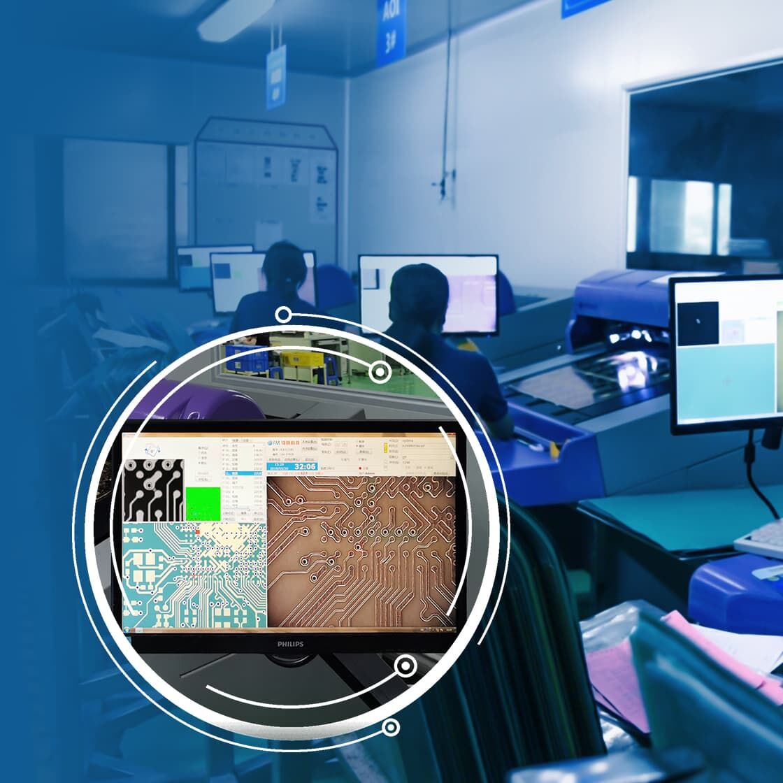
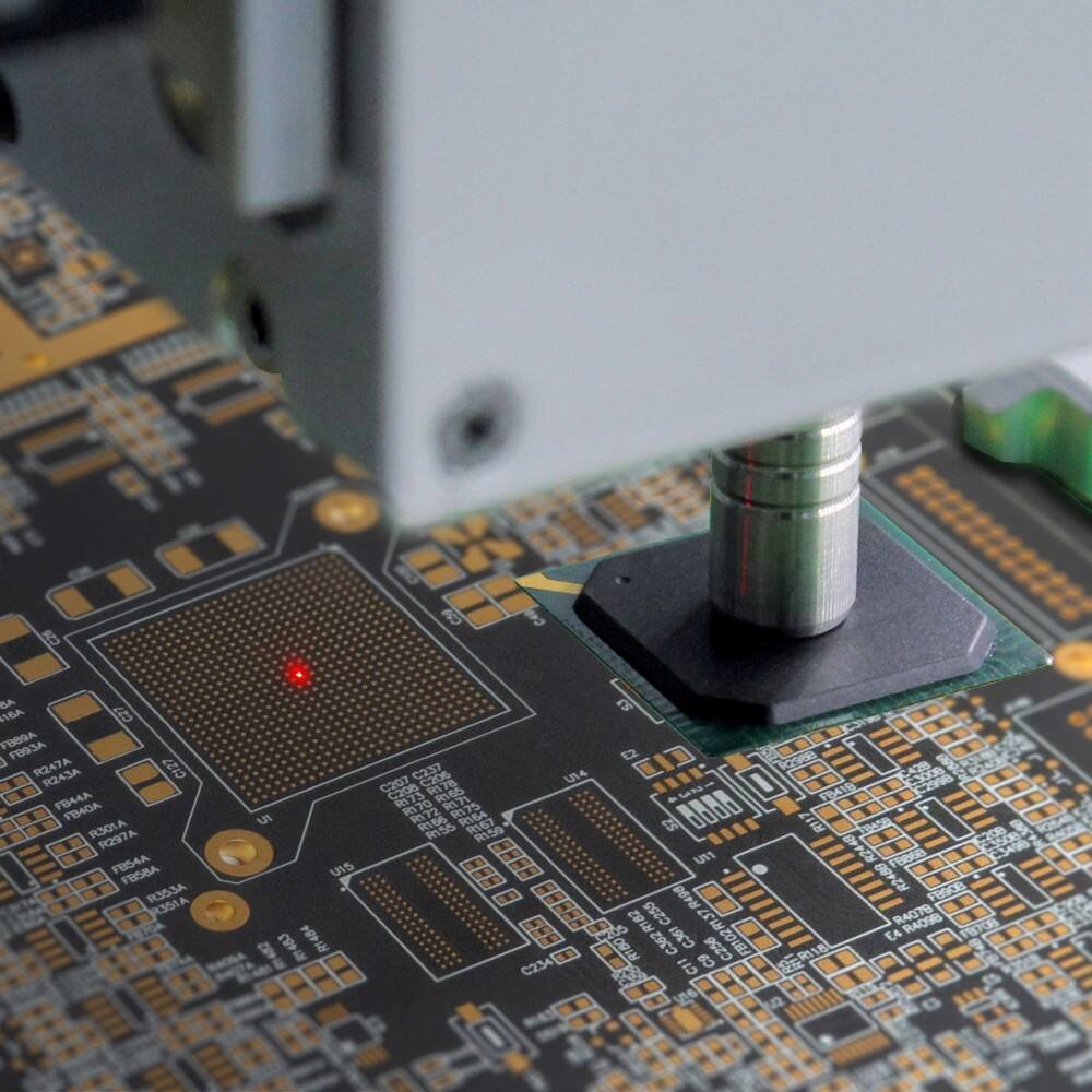
AOI, short for Automated Optical Inspection, is a visual inspection method in which PCB assembly manufacturers utilize cameras and image processing software to identify quality defects on circuit boards. AOI excels in quality control of printed circuit boards (PCBs) and PCB assemblies (PCBAs).
With the rapid advancement of electronic technology, modern circuits are becoming more complex than ever before, and PCBs are moving towards miniaturization and higher density. The market urgently needs reliable and fast inspection methods to meet the quality demands of modern circuits. AOI inspection has become particularly important in PCB manufacturing, ensuring that customers receive high-quality, defect-free boards.
AOI can detect surface defects (scratches), dimensional defects (shorts, opens, thin solder joints), and missing or misplaced components.Inspection content can be divided into two categories:
Line width or spacing discrepancies, missing pads, excess copper, breaks, shorts, damaged gold fingers, damaged holes, incorrect component pads, etc.
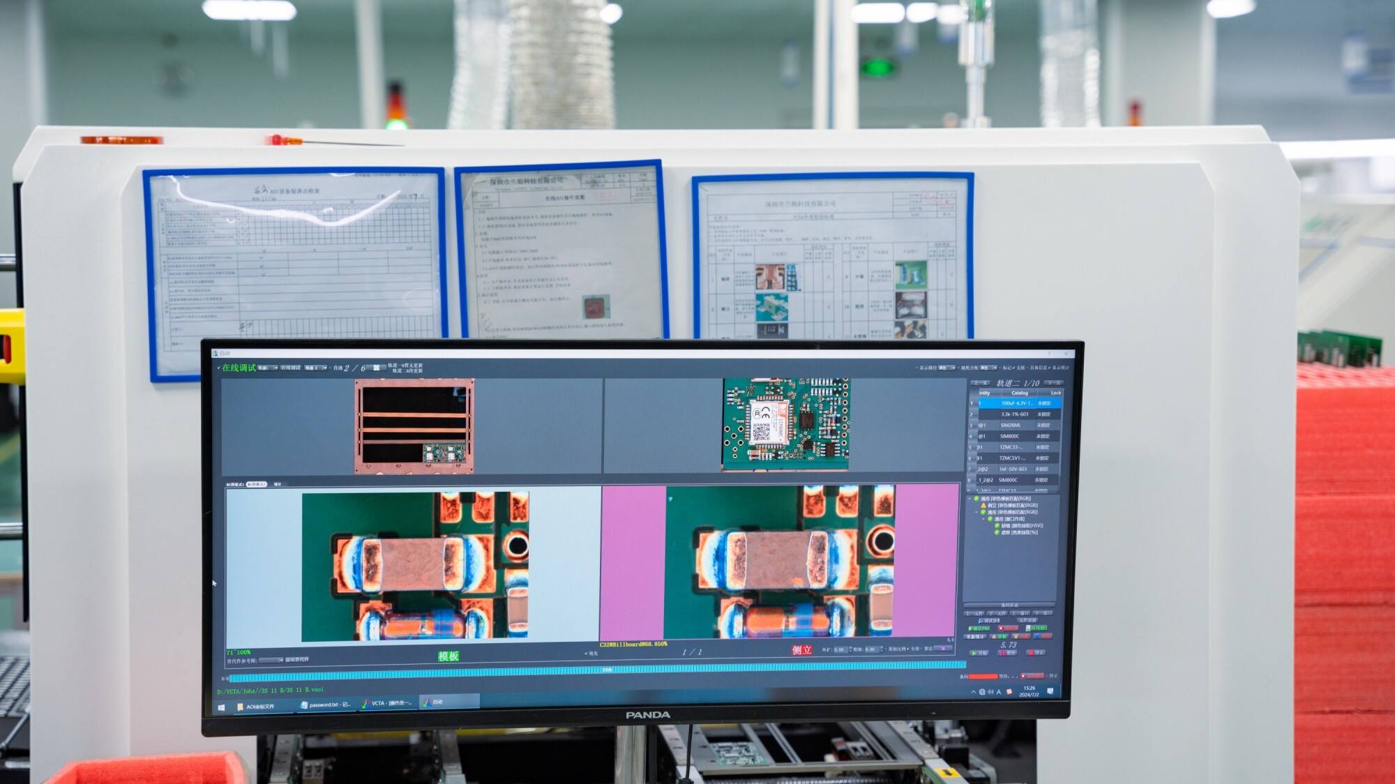
Regional defects, component offset/incorrect polarity/skew, component presence, excessive or insufficient solder joints, abnormal height, flipped components, insufficient solder paste around pins, lifted pins, improper solder volume, and incorrect or damaged components.
AOI is a crucial inspection method for PCBs before they are used in any electronic device. While manual visual inspection was often relied upon in the past, the increasing complexity of PCBs makes manual inspection insufficient for quality assurance. AOI has become a more reliable and faster testing method, offering numerous advantages:
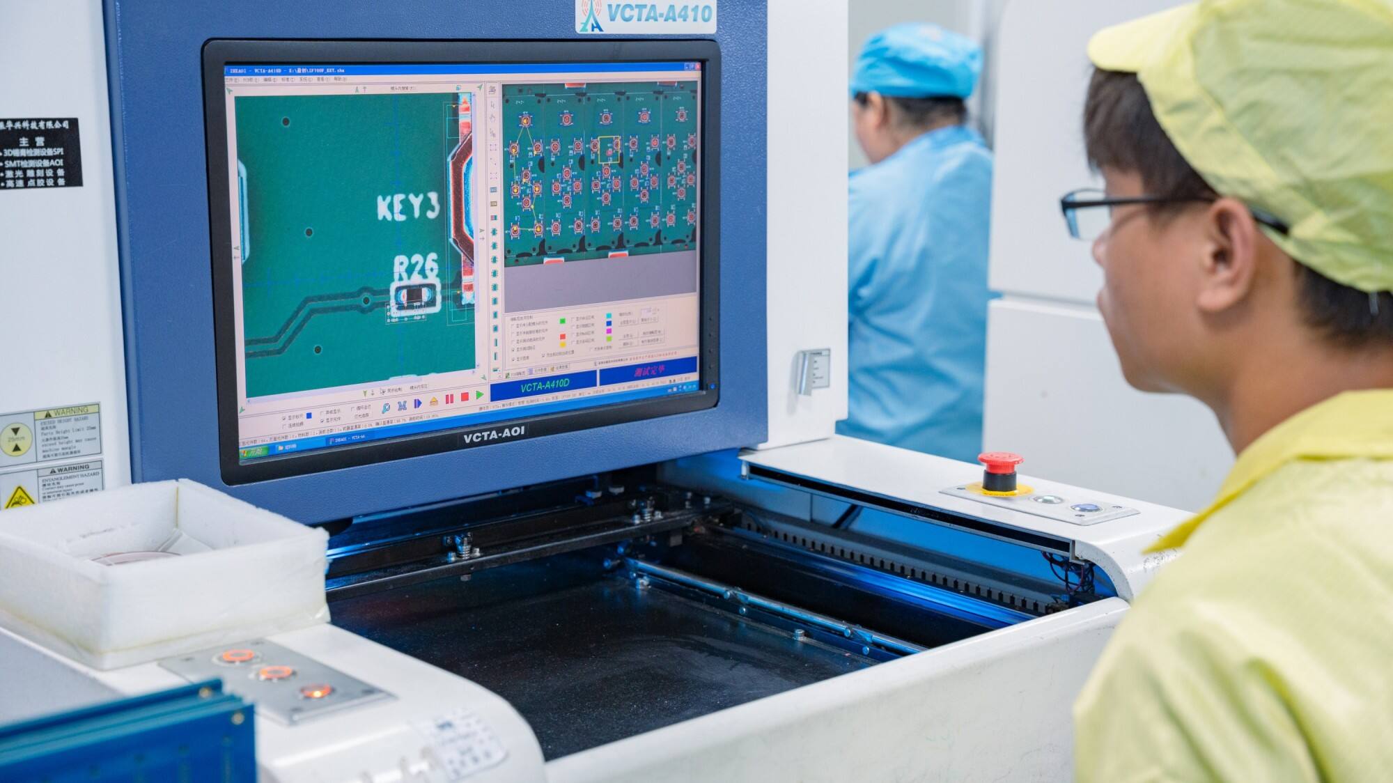
AOI places the circuit board under a high-intensity light source, where one or more high-definition cameras visually scan it and compare the captured image with an ideal image, providing highly accurate inspection results.
AOI is less expensive than other inspection methods, such as X-ray. Furthermore, AOI helps prevent recurring defects, improves production value, and provides long-term benefits to PCB manufacturers.
AOI's greatest advantage is that it can be applied at any stage of the PCB manufacturing process, depending on needs and cost, and can be repeated multiple times.
AOI can be used to inspect both PCBs and PCBAs. It can accurately detect surface defects on individual boards as well as component-related defects, such as soldering quality, numerical identification, and polarity orientation.
AOI is a crucial component of the PCB manufacturing and circuit board inspection process, applicable to PCB manufacturers, assemblers, and service providers. It can detect quality issues on boards produced on the production line and promptly correct them. X-ray inspection is also an indispensable auxiliary tool in PCB manufacturing. NEXTPCB is equipped with advanced inspection equipment to strictly enforce quality standards throughout the PCB manufacturing and assembly process.
Aoi
BGA Assembly
Via-in-Pad
Via Covering