Quick Links
Home > PCB Manufacturing > Drills & Throughplating > Via-in-Pad
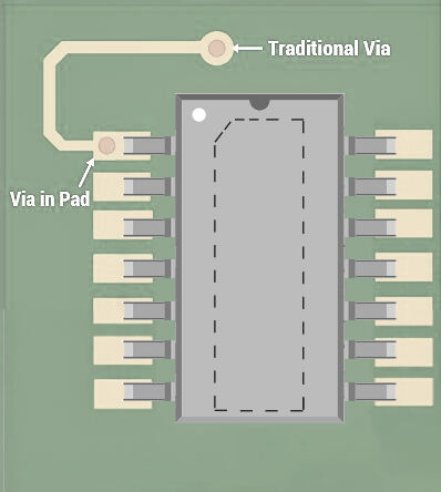
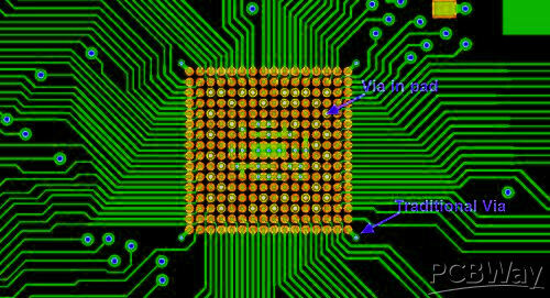
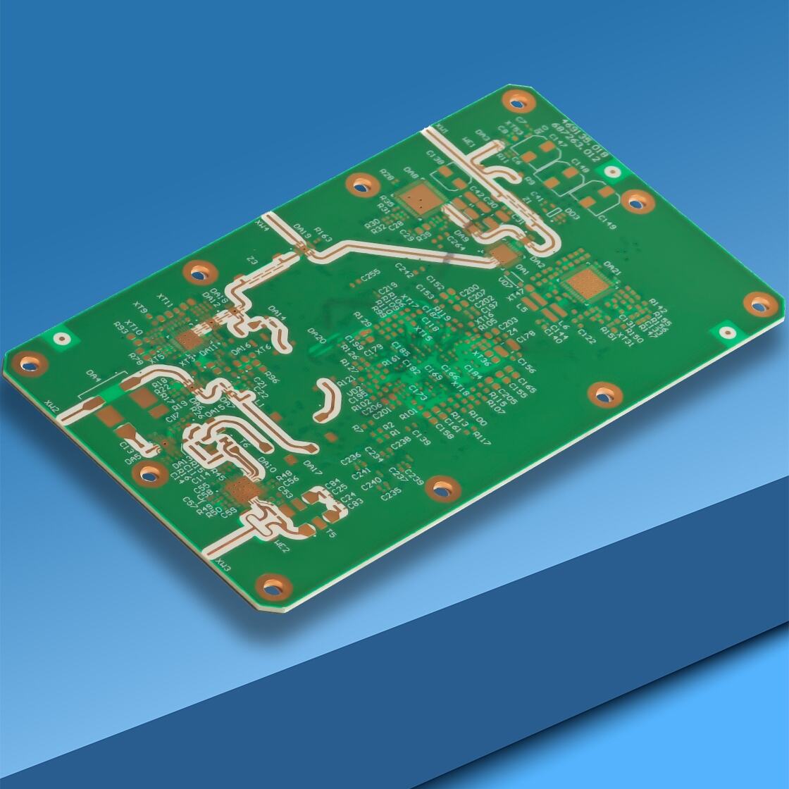
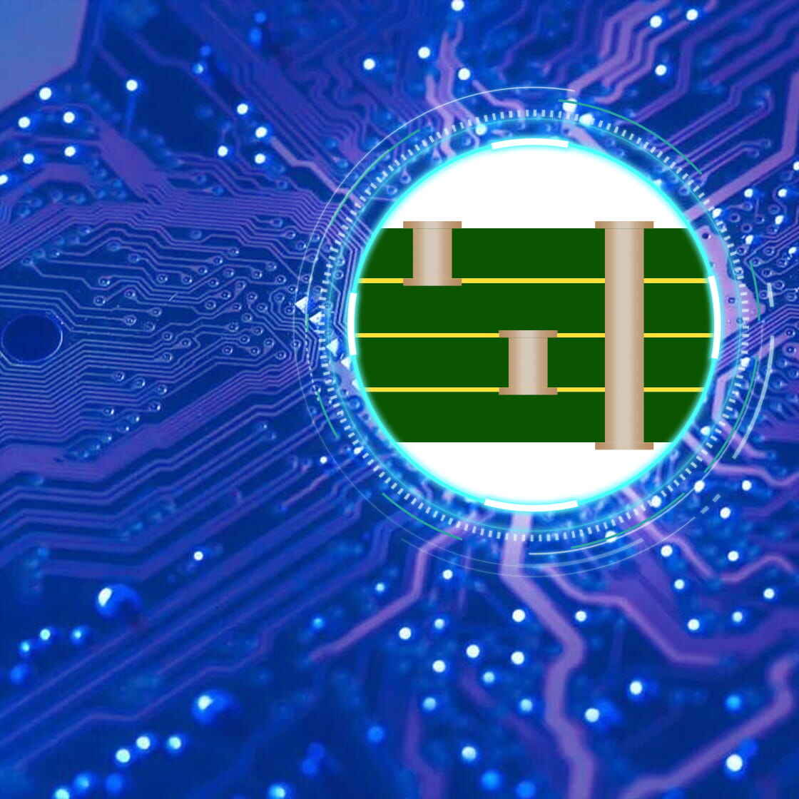
Via-in-Pad is an advanced through-hole technology used in high-density PCB design. Its core feature is to integrate the plated through-hole (PTH) directly into the pad of the surface mount component, achieve electrical connection by depositing conductive materials such as copper in the through-hole, and cover the hole with solder mask to ensure welding reliability.
Unlike traditional through-holes, traditional PTHs are usually arranged in non-welding areas outside the component pads and need to be connected to the pads through additional traces; while Via-in-Pad omits this part of the transition structure, allowing the through-hole and the pad to be directly integrated. This design is like opening a "direct channel" in the center of the pad, which can significantly shorten the signal transmission path and reduce signal delay and loss. From the perspective of practical value, the advantages of via-in-pad are concentrated in two aspects: space utilization and performance improvement: by embedding the through-hole into the pad, the wiring space on the PCB can be reduced, which helps miniaturize the product; at the same time, the shortened signal path can reduce the risk of impedance mutation and improve signal integrity.
However, this technology places higher demands on the manufacturing process: it is necessary to precisely control the drilling accuracy (hole diameter is usually ≤0.3mm) and the uniformity of electroplating to ensure reliable connection between the copper layer of the hole wall and the pad; some designs also require the holes to be filled with resin and flattened to avoid bubbles or cold solder joints during welding. Therefore, its manufacturing cost is higher than that of traditional PTH, and it is usually preferred in scenarios with high density and high performance requirements.
The application of via-in-pad needs to be comprehensively judged in combination with PCB layout density and component characteristics. The following are design recommendations for specific scenarios:
After completing the fan-out design in the early stage of PCB routing, if the inner layer routing can be achieved through conventional vias, there is no need to use via-in-pad. Taking BGA packaged devices as an example, when the fan-out path is located in the central area between pads, efficient routing can be achieved by optimizing via and routing parameters. The typical design standards are as follows:
Based on the above parameters, when the BGA pin spacing is greater than 0.35mm, the space between pads is sufficient to accommodate conventional vias and routing, and fan-out can be completed without relying on via-in-pad. At this time, choosing a traditional design can better balance cost and process reliability.
When the component pin spacing is too small, making it difficult to achieve conventional fan-out, via-in-pad becomes a necessary choice. For example, the space between pads of high-density BGA packages is narrow, and conventional vias and traces cannot be arranged due to size limitations. At this time, the vias need to be directly integrated into the pads, and the inner or bottom layer wiring channels are opened through Via-in-Pad to avoid signal delays or layout failures caused by wiring congestion.
In short, the core application of via-in-pad is to solve the "wiring bottleneck under high-density layout". When designing, it is necessary to first evaluate the feasibility through pin spacing and fan-out parameters, and then decide whether to adopt it to achieve the optimal balance between performance, cost and manufacturability.
For low-pin-count BGA devices, conventional fan-out design can meet the wiring requirements without relying on Via-in-Pad. However, when BGA has a large number of pins, a large number of fan-out vias will quickly occupy the limited wiring space, resulting in congestion in the signal path. At this time, integrating the vias into Via-in-Pad can combine the originally independent "pads + vias" into one, significantly freeing up the PCB surface space and creating conditions for high-density wiring.
Especially when the BGA pin pitch is reduced to less than 0.3mm, there is no enough space between the pads to accommodate conventional vias and traces, and Via-in-Pad becomes a key means to break through the wiring bottleneck. By embedding the vias inside the pads, the signal can be directly guided to the inner or bottom layers to avoid signal delays or cross-interference caused by crowded wiring on the same layer.
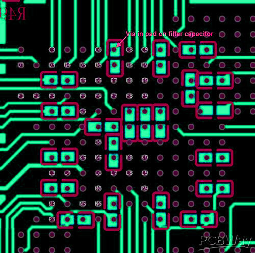
In high-speed circuit design, filter capacitors are usually placed close to BGA devices to suppress power noise and ensure signal integrity. However, if a large number of conventional through-holes are used inside the BGA, the through-hole area on the back will "compete for territory" with the capacitor pads, resulting in the inability to place the capacitor close to the chip pins.
Via-in-Pad can completely avoid spatial conflicts with the back capacitors by integrating through-holes into the BGA pads, ensuring that the filter capacitors can be "closely" placed under or at the edge of the BGA, shortening the power path and improving filtering efficiency. This is crucial to the stability of high-frequency and high-speed circuits.
1. Ultimately release PCB wiring space: The integrated design of through-holes and pads can reduce surface space occupancy by more than 30%, which is especially suitable for high-density, miniaturized designs such as smartphone motherboards and industrial control modules.
2. Enhance heat dissipation and electrical performance: For high-power devices such as processors and power chips, Via-in-Pad can reduce thermal resistance, accelerate heat conduction to the inner layer or heat dissipation layer, and avoid local overheating; at the same time, the shortened power/signal path can reduce parasitic inductance and resistance, reduce signal attenuation and voltage drop.
3. Improve layout flexibility: Solve the pain point of "insufficient wiring channels" under high-density packaging, making the layout of complex circuits such as multi-channel RF modules more relaxed.
1. Increased process complexity: Special processes such as hole filling and surface flattening are required, which require higher drilling accuracy and electroplating uniformity, and are prone to defects such as bubbles in the holes and surface depressions.
2. Increased manufacturing costs: Special processes will increase PCB costs by 15%-30%, and the production cycle will be extended due to additional quality inspections and rework.
Rogers PCB
Blind & Buried Vias
Plated-through Slots
Box Build Assembly