Quick Links

Home > PCB Manufacturing > Printed Circuit Board > Flexible PCB
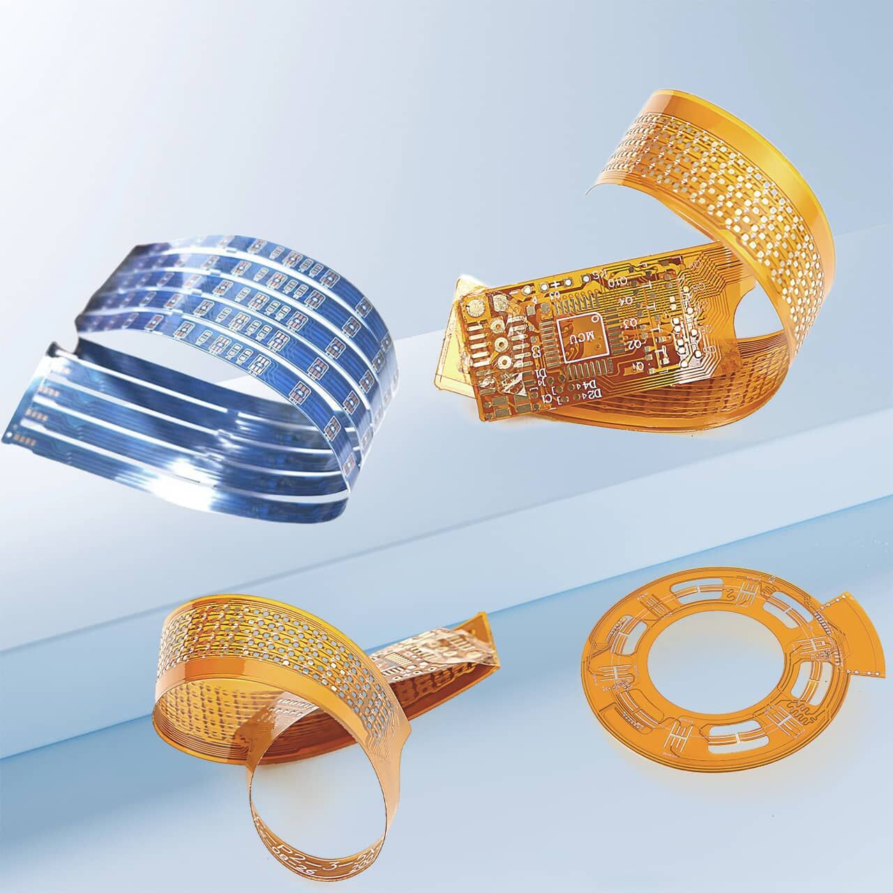
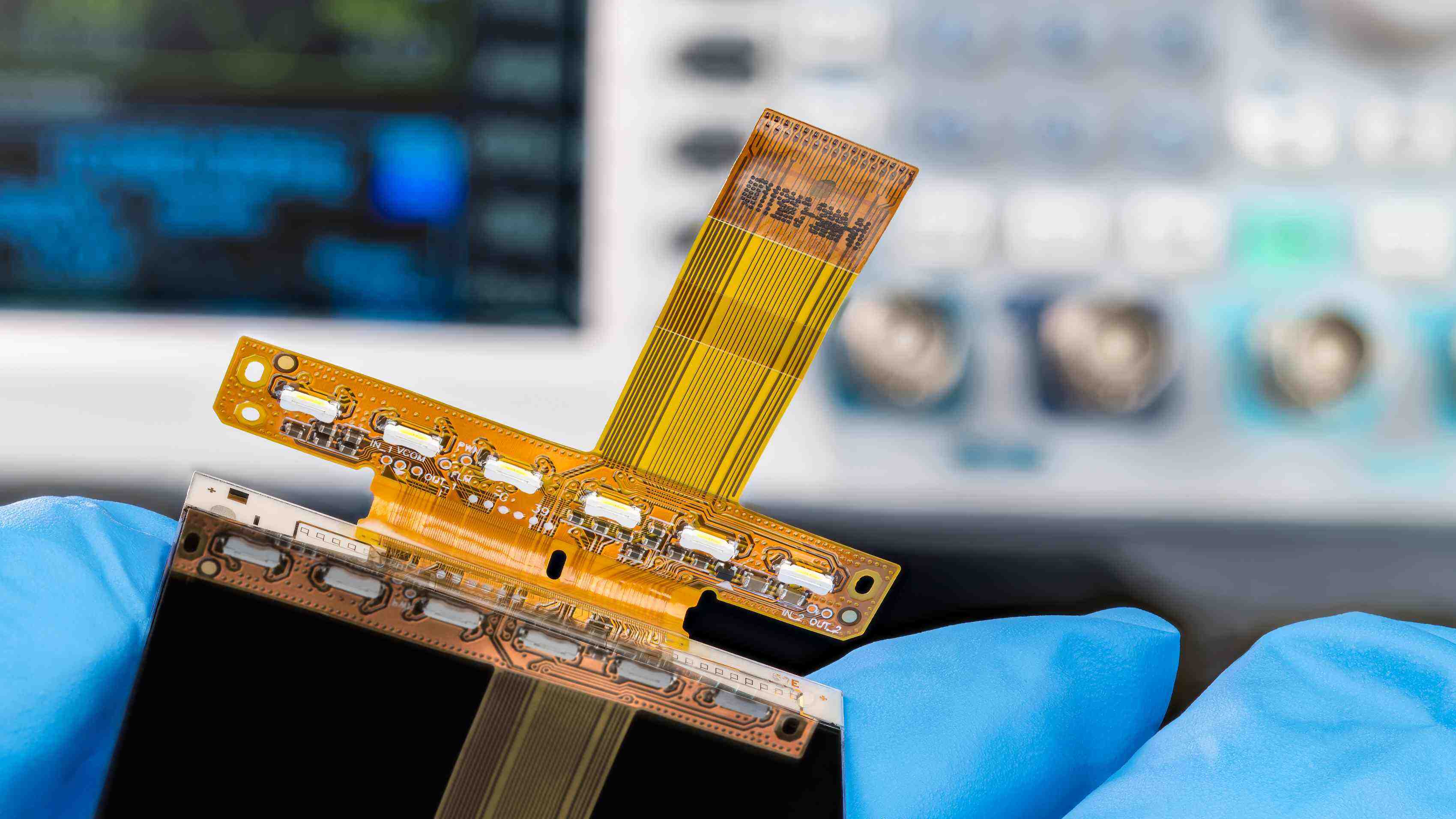
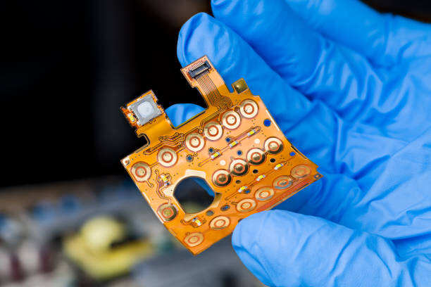
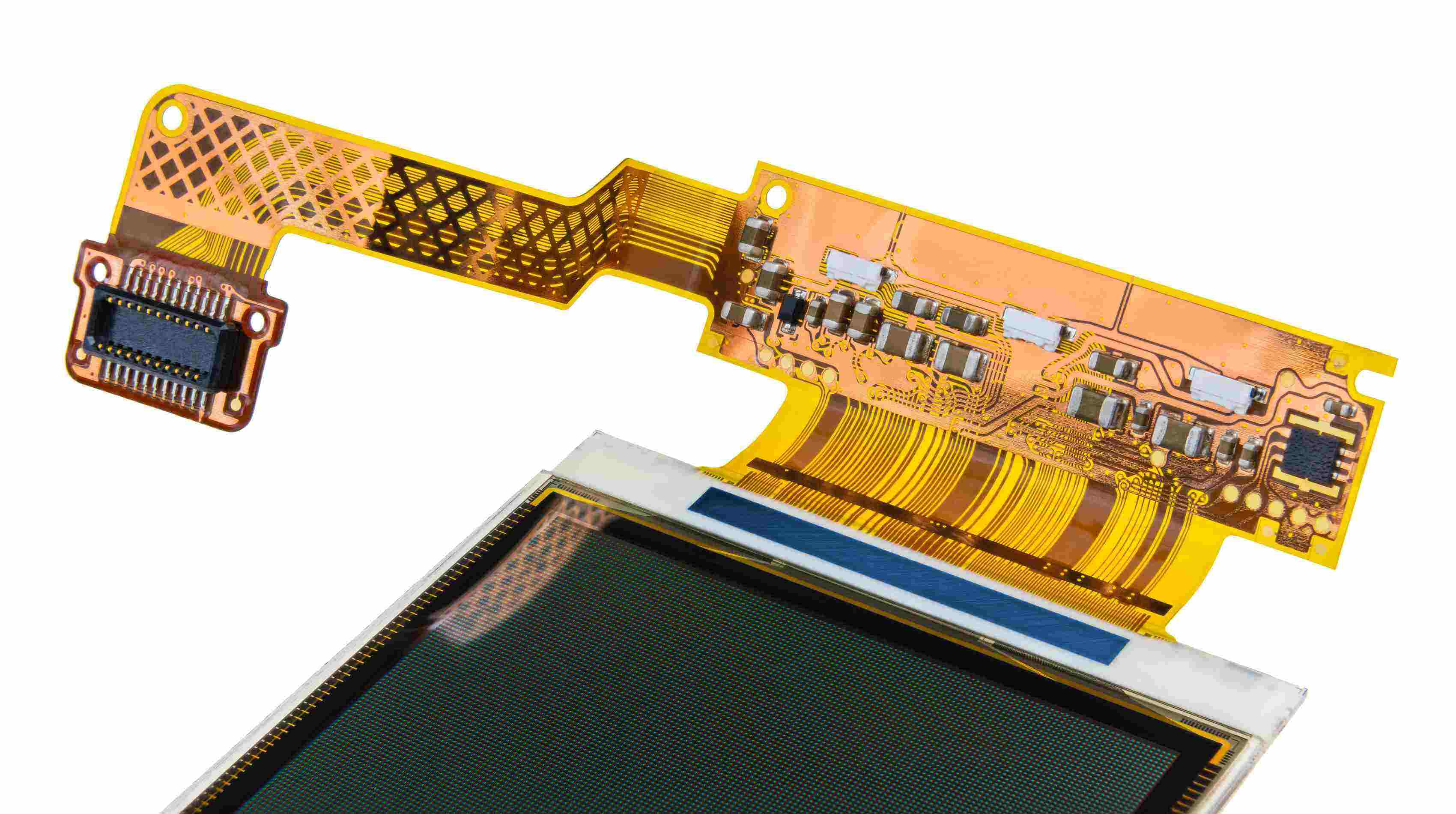
Flexible printed circuit boards (Flexible PCBs) can be bent to fit into narrow or dynamic spaces. They are constructed with a copper layer placed on a flexible substrate film to miniaturize the device. They are commonly found in cameras, smartphones and medical devices. The bending properties provide layout flexibility while ensuring signal transmission reliability.
Flexible printed circuit can reduce the size and weight of devices, making products thinner and lighter, and improving the comfort and durability of wearable devices. They reduce cables and connectors, simplify assembly processes and improve production efficiency. Flexible PCBs are resistant to movement and stress and are widely used in electric vehicles, drones, smart homes and other fields, promoting the advancement of manufacturing technology.
The following content covers the main types, structures, advantages and disadvantages of flexible PCBs, and compares them with rigid PCBs.
Flexible circuit board is a thin circuit board with a flexible film as the substrate, carrying copper wires for power and signal transmission. The substrate can be wrapped, conformed or bent to adapt to space constraints. flexible pcb board is an ideal choice when rigid PCB cannot meet space or dynamic requirements.
Compared with rigid PCB, which uses a hard substrate, flex pcbs can be bent to adapt to device movement or compact space, reduce connectors and cables, reduce weight and simplify assembly.
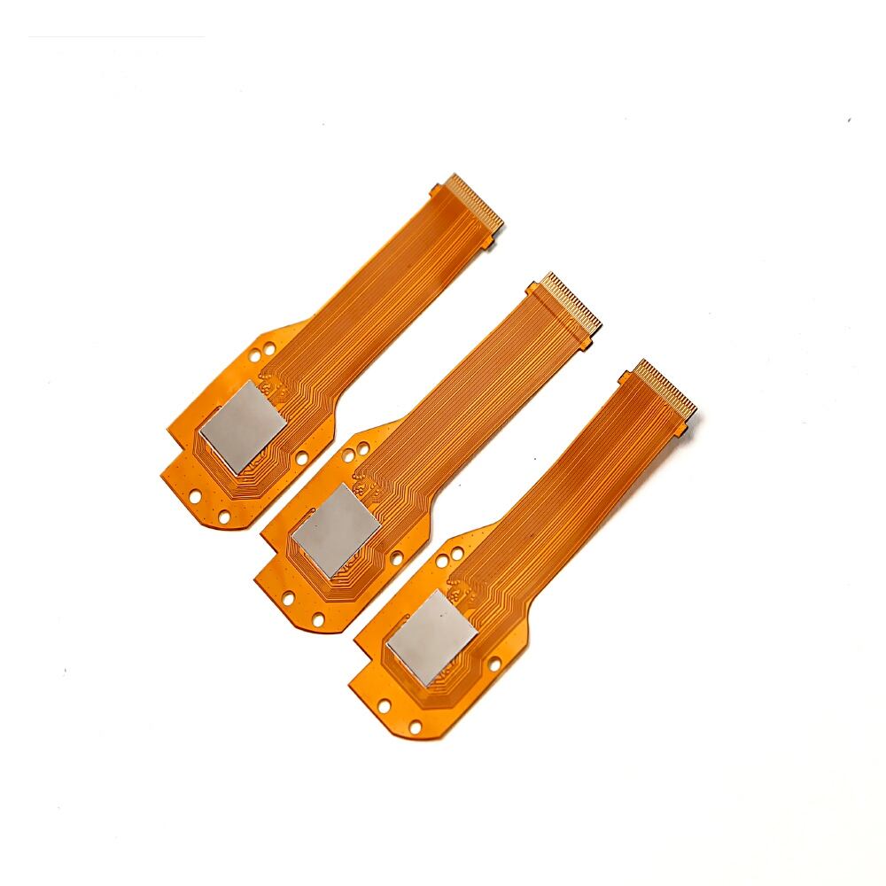
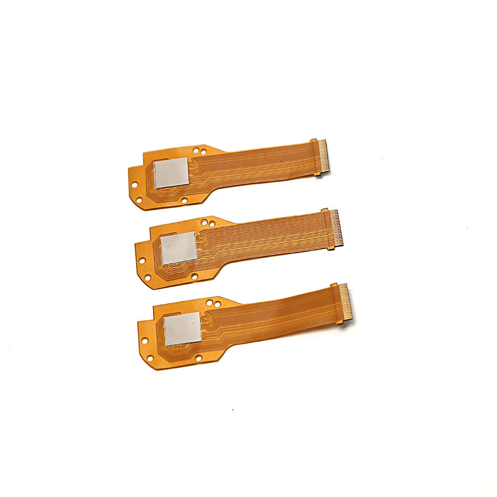
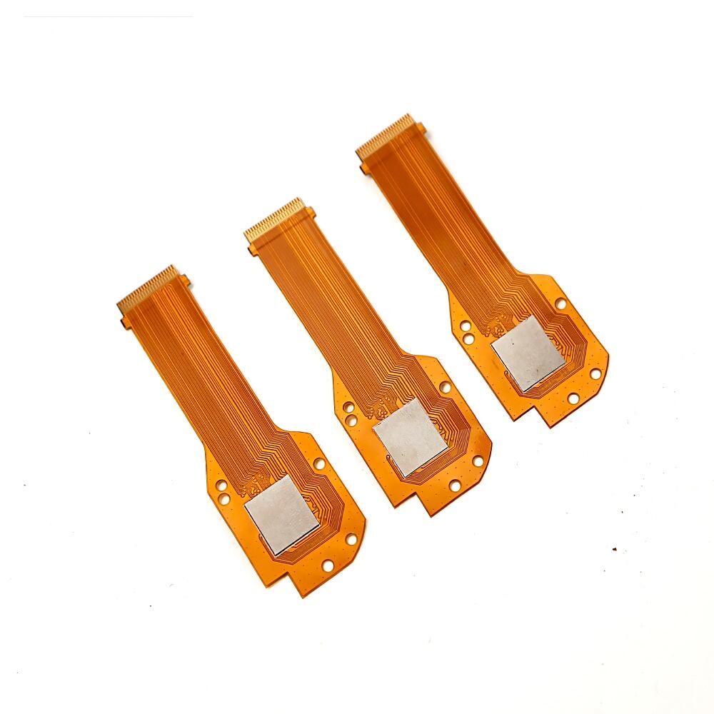
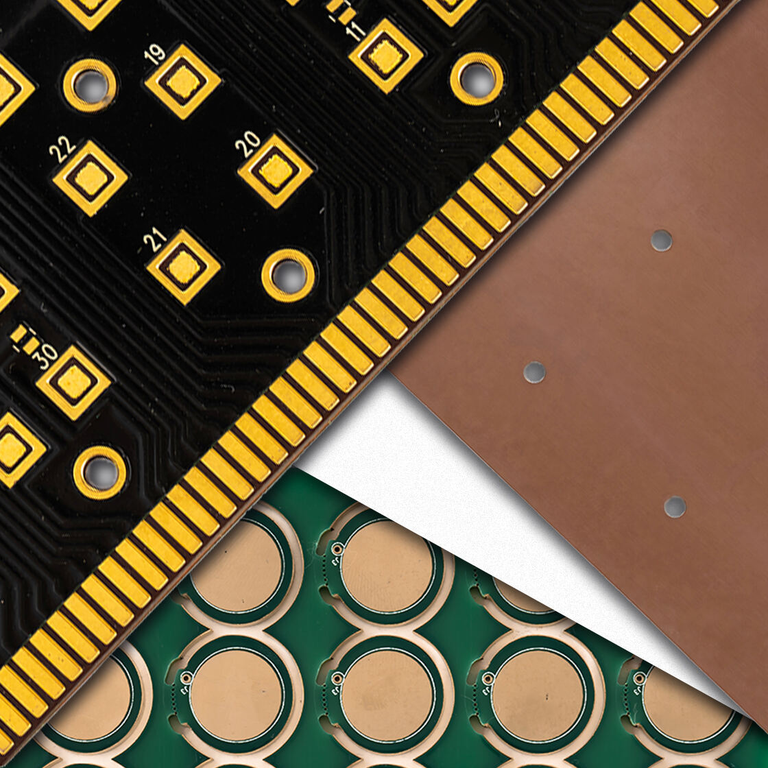
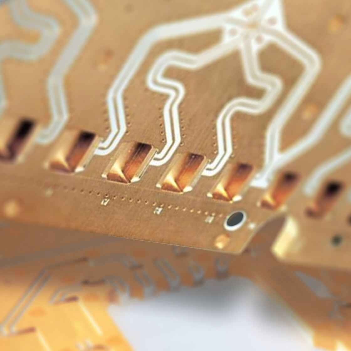
Flexible PCB often uses polyimide or polyester film as the substrate. Copper foil is laminated to the substrate with adhesive, and the coverlay protects the wires and maintains the bending ability. Stiffeners are used to locally support components, and coverlays are used to improve insulation and strength. The number of layers and thickness are adjusted according to the application requirements to balance flexibility and durability. It has a wide range of applications, such as cameras, mobile phones, wearable devices, sensors, medical scanners, smart glasses, and drones. The automotive industry uses it for dashboards and sensors; aerospace uses it for its lightweight and bendability; it is also applicable to robots with moving parts.
Feature |
Capability |
| Substrate |
Polyimide Polyester PTFE |
| Layer Count | 1~12 layers |
| Substrate Thickness | 12~125 μm |
| Copper Thickness | 12/18/35/70 μm |
| Coverlay | PI+Adhesive~25~50 μm |
| Single Layer Thickness | 0.08~0.2 mm |
| Multi-Layer Thickness | ≥0.15 mm |
| Minimum Line Width | 3~5 mil(0.075~0.127 mm) |
| Minimum Line Distance | 3~5 mil(0.075~0.127 mm) |
| Minimum Mechanical Aperture | 0.15~0.2 mm |
| Minimum Laser Aperture | 0.1 mm |
| Solder Mask | ≥3 mil(0.075 mm) |
| Coverlay Clearance | ≥3 mil (0.075 mm) |
| Surface Finish | ENIG, OSP, Immersion Tin/Silver |
| Heat Resistance | 260℃/20s |
| Dk | 3.2~3.5(@1MHz) |
| Df | ≤0.02 |
| Flex Life | ≥100,000 times |
| Dimensional Tolerance |
±0.1 mm (outline) ±10% (thickness) |
| Finished Product Packaging |
Foam Bubble Pad Anti-static bags |
Flex circuit board come in many varieties and are widely used in electronic components and devices. Here are some specific introductions:
Copper circuits are arranged on only one side of the substrate. The polyimide film carries the signal, and the cover film provides protection and bend identification. The structure is ultra-thin and low-cost, suitable for basic circuits. Typical applications are sensor wiring, LED light strips, and basic signal connections. Usually only one-time bending or keeping straight is required to reduce wiring harnesses and weight. Simple manufacturing, suitable for small batch production. The disadvantage is that the wiring capacity is limited, complex wiring requires jumpers or external wires, single-layer wiring needs to avoid crossing, and the reinforcing plate increases the thickness.
Copper circuits are arranged on both sides of the substrate, and interlayer interconnection is achieved through through holes or microvias. The wiring density is higher at the same size, and the double-sided cover film is protected. Keep it light and thin, and handle medium-complexity signals. Typical applications are barcode scanners, camera wiring, and LED backlight panels. The advantage is that the power and signal lines are separated, and the wiring is more flexible. The disadvantage is that the manufacturing process (drilling, electroplating) is more complicated and the cost is higher than that of a single-sided board. The key point of the design is to avoid arranging through holes in the bending area; follow the bending area design rules provided by the manufacturer (such as wire width and spacing) to ensure long-term reliability.
Contains three or more copper conductor layers, separated by flexible insulation layers. The inner layer can be arranged with power layer and ground layer to reduce noise. Interconnection through blind or buried holes saves space. Overall cover film protection. Suitable for high-speed circuits, RF modules, and small camera module connections. The advantage is that the power, ground, and signal are integrated into a thin structure, with good signal integrity and strong anti-EMI capability. The disadvantage is high manufacturing cost and complex process. The key point of the design is that the number of layers determines the thickness and process; the key signals are arranged in the inner layer; the increase in the number of layers requires an increase in the minimum bending radius, and it is necessary to balance reliability and flexibility.
All flexible designs are based on flexible substrates. Static flexible boards are used in scenarios where only one-time installation and bending are required (such as cameras and mobile phones) with low cost. Dynamic flexible boards are used in locations that require repeated bending (such as hinges and folding screens). This needs to be designed specifically to withstand thousands of bending cycles: reduce copper wire stress and set a neutral bending line. Material selection (substrate, cover film, copper thickness) depends on bending requirements and cost budget.
Flexible PCB with reinforcement plate, the reinforcement plate (material: FR4, polyimide, metal sheet) is fixed to a specific area of the flexible board by adhesive. The function is to support heavier components (such as connectors, chips), enhance local flatness and strength, and prevent solder joints from cracking due to bending. The application location is the connector pad, under the component, board edge, and test point. Its design points are that the reinforcement plate area needs to be reserved to avoid affecting the adjacent bending area, the bonding needs to be strong and heat-resistant, the transition zone cover film needs to be smooth, and the local thickening needs to consider assembly and welding process adjustments.
Integrate the rigid board area and the flexible area in a single structure. The flexible layer is pressed into the rigid part during manufacturing. Its advantage is that no additional cables are required to connect the rigid area; local rigid support is provided, flexible connections are retained, weight is reduced, space is saved, and assembly is simplified. Mainly used in aerospace, medical implants, and military equipment. Specific requirements are high-precision lamination and alignment technology. Its design key points are to define mechanical fit and bending paths in the early stage; CAD tools are required to support hybrid structure design.
The core is a flexible substrate film (such as polyimide). Copper foil is laminated on it to form the circuit. Adhesive ensures that the copper layer is bonded to the substrate. Cover film is used as an outer layer to provide moisture and wear protection and extend the flex life.
The bending radius is a measure of the maximum bending capacity of flexible boards. The common rule is "bending radius ≈ board thickness × 10". For example: a board with a thickness of 0.1mm has a minimum bending radius of 1mm.
A smaller radius (such as thickness × 5) is allowed for one-time bending.
If it is repeated bending, the minimum radius must be strictly followed, otherwise it is easy to cause material fatigue fracture. The material affects the performance. Polyimide is heat-resistant and resistant to repeated bending, and polyester is low-cost and suitable for static applications. The thinner the copper foil, the better the flexibility.
The main function is to provide local flatness and mechanical support for pads (connectors, components, test points). Prevent solder joints from cracking due to bending stress. Heat-resistant adhesives are required for firm bonding.
Materials used: FR4 (low cost), polyimide (good thermal matching), aluminum sheet (high strength). Stiffeners require precise cutting and edge treatment (such as tape/covering film wrapping) to prevent peeling.
Wiring planning: Determine the wire width (affects current carrying and rigidity) and spacing (avoid bending short circuit) as early as possible. The wires in the bending area should be smooth curves.
Bending area processing: Avoid key signal lines and through-holes. Key networks are laid out in stable areas.
Component placement: Place them in non-bending areas first. If they are close to the bending area, consider using flexible connectors or ZIF sockets.
Design tools: Use CAD tools that support flexible design, with stacking modeling, stress analysis, and bending simulation functions, to facilitate collaboration with mechanical design.
Flexible PCB technology expands design possibilities through space saving, weight reduction and assembly simplification. Choose single-sided, double-sided, multi-layer or rigid-flex boards according to your needs. Ensure its reliability in dynamic applications through reasonable material selection, wiring planning and bending design.
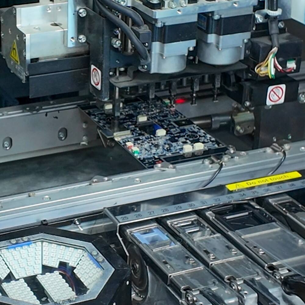
Manufacturers such as PCBally provide expertise, fast prototyping and mass production support. Choosing the right type of flexible board helps to efficiently and reliably develop thin and light electronic devices with moving parts.
Silkscreen
Copper Based PCB
Smt Assembly
Teflon PCB