Quick Links

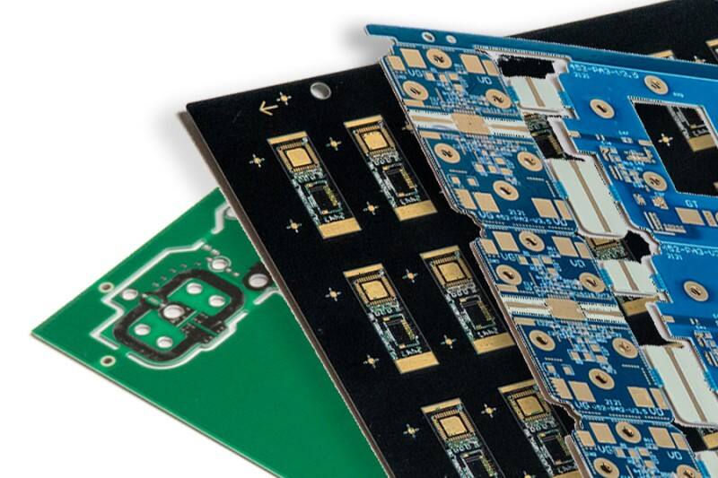
The solder mask (also called solder mask) is a thin layer of polymer material applied to the surface of the PCB (printed circuit board). Its main function is to protect the copper traces and prevent solder from flowing into areas where soldering is not required during soldering. In order to make the soldering more perfect, the entire circuit board, except for the pad area, will be coated with a solder mask.
Solder mask is applied on both sides of the PCB. Resin is the main component of solder mask because it has good moisture and high temperature resistance and is non-conductive. Initially, most PCBs used green solder mask, so it is often called "green oil". However, solder mask also has many colors, such as green, white, yellow, red, blue, black, etc. The specific color to use depends on the different needs of customers.
There are different types of solder mask on PCB. Regardless of the type, it needs to be heat cured after the pattern is determined. Common types of solder mask are as follows:
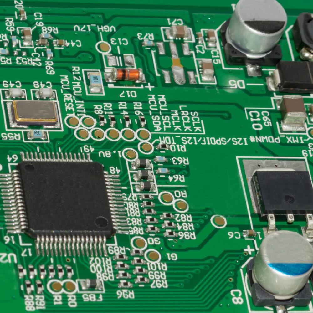
Solder mask is a key process in PCB manufacturing. The colored surface layer on the PCB is the solder mask. The solder mask is a "negative output", so when the solder mask pattern is applied to the board, the copper is exposed in the pattern opening instead of being coated with solder mask ink.
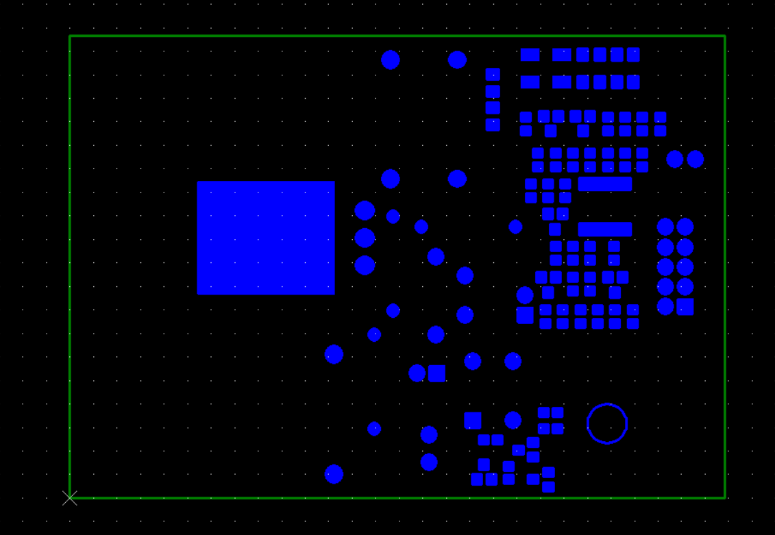
The steel mesh layer is actually a template for SMD device packaging, corresponding to the pads of SMD components. It can be directly understood as a steel sheet mold designed and made according to the steel mesh layer. In the SMT mounting process, a steel mesh is usually used to punch holes at the corresponding positions of the PCB pads, and solder paste is scraped on the steel mesh. When the PCB is placed under the steel mesh, the solder paste will flow down through the holes and evenly cover the pads. Therefore, the opening of the steel mesh layer should not be larger than the actual pad size, and it is better to be slightly smaller or equal to the pad.
Usually, we can only manufacture single-layer aluminum substrates and double-layer aluminum substrates. Due to the limitations of the manufacturing process, multi-layer aluminum substrates are difficult to manufacture, so they cannot meet the needs of complex multi-layer designs.
Metal aluminum materials have high rigidity and low softness, and are not as flexible as polyimide or polyester substrates. Therefore, they are not suitable for applications that require repeated bending.
The thermal expansion coefficient of aluminum substrates is relatively high, which is different from some components and solder materials. The mismatch of the thermal expansion coefficients of the two can easily lead to solder joint damage or delamination, affecting overall reliability.
Compared with ordinary substrates, the metal properties of aluminum substrates require more time to consider during manufacturing and assembly, which will increase process complexity and cost.
Although aluminum substrates have significant advantages in thermal management, compared with traditional FR4 materials, aluminum-based PCBs have higher material costs, special manufacturing processes and surface treatment requirements, so the overall manufacturing cost increases.
Fr4
Reverse Engineering
Quick Turn PCB Assembly
BGA Assembly