Quick Links
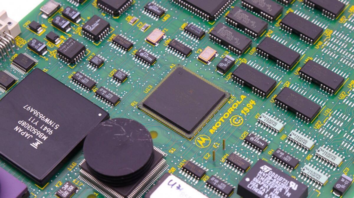
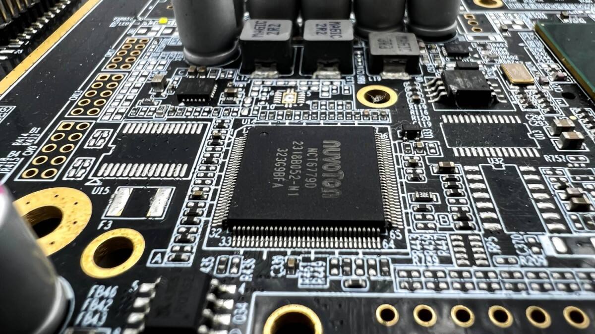
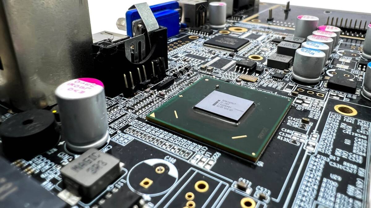
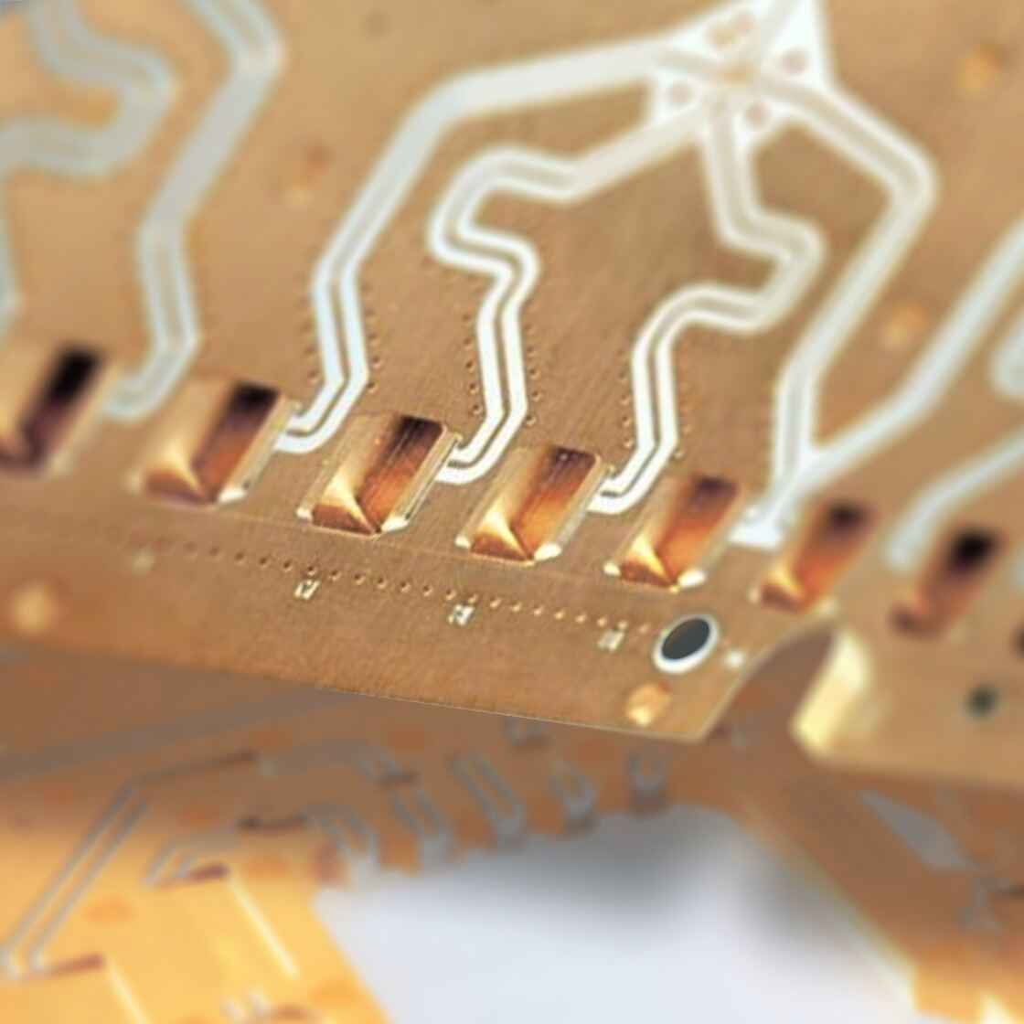
BGA (Ball Grid Array) is an integrated circuit package designed for high-density circuits. Its core feature is a grid-like pattern of tiny solder balls arranged on the bottom of the package. These solder balls replace the pins of traditional packages, acting as an electrical bridge between the chip and the PCB, responsible for signal transmission and power supply, and also as a key mechanical connection. Compared to pin-based or conventional surface-mount packages, BGAs can achieve hundreds or even thousands of connection points within a limited space. Therefore, they are widely used in high-frequency processors, memory chips, and other applications that require extremely high speed, power, heat dissipation, and electrical performance.
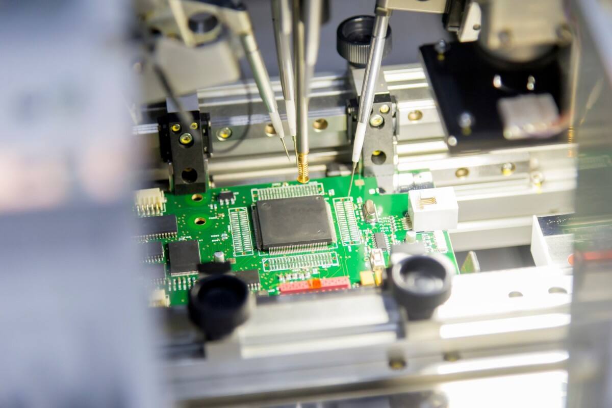
BGA assembly involves precisely attaching these BGA chips with bottom solder balls to a PCB through an automated soldering process. Because the solder balls directly bond to corresponding pads on the PCB, the bending structure of traditional pins is eliminated. This not only shortens the signal path and reduces interference, but also reduces thermal resistance and improves heat dissipation efficiency through a compact design.
Unlike traditional SMD packaging, BGA assembly relies entirely on automated equipment, such as high-precision placement machines and reflow ovens. From solder paste printing to final inspection, strict precision control is required. This is necessary to cope with high-density connections and is crucial for ensuring high reliability. As a result, BGA assembly demonstrates advantages over traditional packaging in electronic devices requiring high-speed processing and high power output.
Cable assemblies of different structures are suitable for different scenarios due to their varying characteristics:
First, matching pads are designed on the BGA soldering area of the PCB. Then, a solder paste consisting of solder and flux is evenly applied to the pads using a stencil. The amount of solder paste used directly affects the quality of the solder joints and must be strictly controlled.
A high-speed automatic placement machine uses a high-definition camera to identify the positioning marks on the chip and PCB. After picking up the BGA chip, it is precisely placed on the printed solder paste, ensuring that each solder ball aligns with the corresponding pad. This step is commonly known as "Pick-and-Place."
The assembled PCB is fed into a reflow oven. As the temperature rises, the solder paste gradually melts and fuses with the solder balls on the bottom of the BGA. After cooling, a strong solder joint is formed, completing the electrical and mechanical connection.
Because the BGA solder joints are hidden on the bottom of the chip and cannot be directly observed, they must be inspected using X-ray equipment to check for shorts, air holes, and cold solder joints. Electrical performance testing is also performed to ensure connection reliability.
BGA assembly requires extremely high process precision, requiring strict control across multiple stages:
BGA assembly is a technical process in electronics manufacturing that requires extremely high precision and experience, demanding meticulous attention to detail, from equipment performance to process details. As a professional service provider, PCBally offers a one-stop service, from engineering assessment, parts procurement, stencil fabrication, to SMT placement, solder inspection, and finished product testing. Whether it's a complex, high-pin-count BGA or a scenario with specialized requirements for heat dissipation or signal transmission, PCBally's standardized processes and customized expertise ensure that every chip forms a stable, reliable, and long-lasting connection to the PCB, laying a solid foundation for the high-performance operation of electronic devices.
Components Sourcing
PCBA Packaging
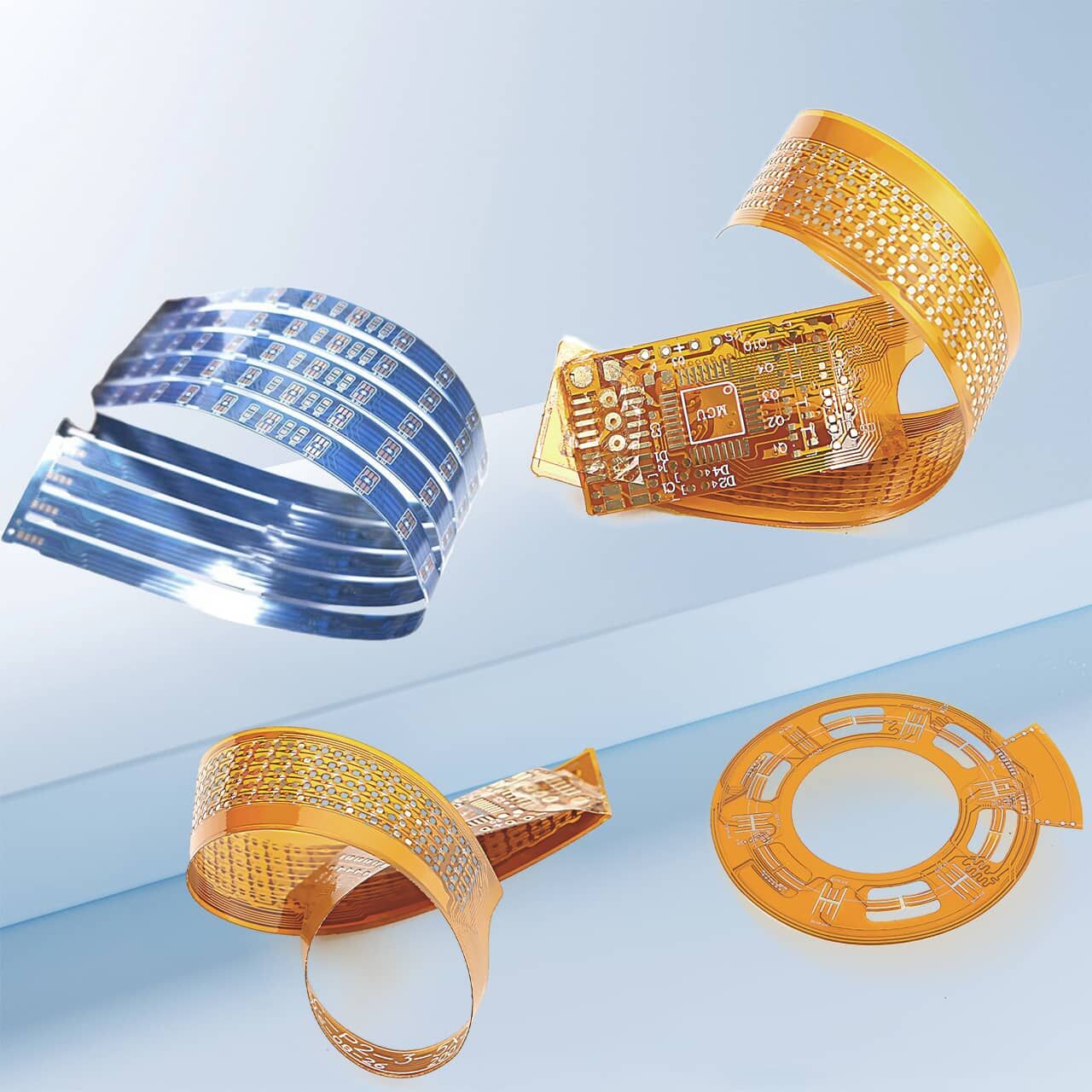
Flexible PCB
Teflon PCB