pcb x ray
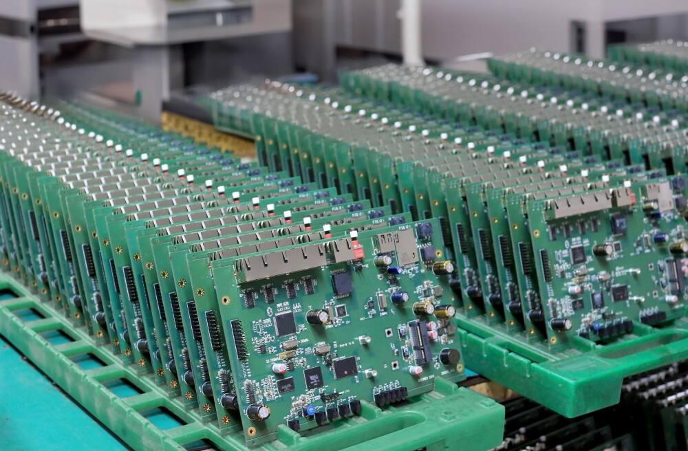
PCB X-ray inspection technology represents a crucial advancement in quality control and analysis within the electronics manufacturing industry. This non-destructive testing method utilizes advanced X-ray imaging to examine printed circuit boards at multiple layers simultaneously, providing detailed insights into their internal structure and composition. The technology operates by penetrating through various PCB layers, generating high-resolution images that reveal potential defects, component placement accuracy, and solder joint quality. Modern PCB X-ray systems feature sophisticated software that enables both 2D and 3D imaging capabilities, allowing inspectors to examine boards from multiple angles and depths. The technology proves particularly valuable in detecting hidden defects such as voids in solder joints, component misalignment, and internal structural issues that would otherwise remain invisible to conventional optical inspection methods. These systems typically offer magnification ranges from 100x to 3000x, providing exceptional detail for both micro and macro-level inspection requirements. The technology has become indispensable in industries requiring high reliability, such as aerospace, medical device manufacturing, and automotive electronics, where component failure could have serious consequences.