

Understanding the Complex Journey of Circuit Board Production
PCB manufacturing has revolutionized the electronics industry, enabling the creation of increasingly sophisticated devices that power our modern world. From smartphones to medical equipment, printed circuit boards serve as the foundation for electronic innovation. This comprehensive guide explores the intricate processes involved in PCB manufacturing, revealing how raw materials transform into precise, functional circuit boards.
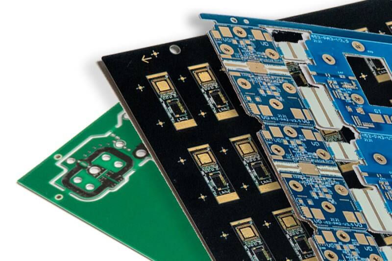
Essential Materials and Components in PCB Production
Base Materials and Substrate Composition
The PCB manufacturing process begins with selecting appropriate base materials. The most common substrate is FR-4, a composite material made of fiberglass reinforced epoxy laminate. This material offers excellent electrical insulation properties and mechanical strength. Manufacturers also use alternative materials like polyimide for high-temperature applications or ceramic substrates for specialized requirements.
The copper foil used in PCB manufacturing plays a crucial role in creating conductive pathways. Available in various weights and thicknesses, the selection depends on the circuit's current-carrying requirements and the overall board specifications. High-quality copper foil ensures reliable electrical connections and optimal performance.
Chemical Solutions and Processing Materials
Several chemical solutions are essential in PCB manufacturing. These include photoresist chemicals for pattern transfer, etching solutions for removing unwanted copper, and plating solutions for adding conductive layers. The quality and composition of these chemicals directly impact the final board's reliability and performance.
Additional materials include solder mask, which protects copper traces and prevents short circuits, and silkscreen ink for component labeling and identification. These finishing materials contribute to both the functionality and usability of the completed circuit board.
The Step-by-Step Manufacturing Process
Design and Layout Preparation
Before physical PCB manufacturing begins, engineers create detailed designs using specialized CAD software. This crucial step involves component placement, trace routing, and layer stack-up planning. The design must account for electrical requirements, thermal considerations, and manufacturing constraints.
Once the design is complete, it undergoes extensive verification and optimization. Design for Manufacturing (DFM) checks ensure that the board can be produced efficiently and reliably. Any potential issues are addressed before moving to production.
Layer Processing and Imaging
The PCB manufacturing process continues with the preparation of individual layers. Photoresist is applied to copper-clad laminate sheets and exposed to UV light through film artwork. This creates a precise pattern that protects copper areas needed for circuits while leaving unwanted areas exposed.
Advanced PCB manufacturing facilities use direct imaging systems for increased accuracy and repeatability. These systems eliminate the need for film artwork and reduce potential alignment errors, resulting in higher quality boards.
Advanced Manufacturing Techniques
Surface Treatment and Plating
Modern PCB manufacturing incorporates sophisticated surface treatment processes. After etching removes unwanted copper, boards undergo electroless copper plating to create conductive through-holes. This is followed by electrolytic copper plating to build up conductor thickness.
Surface finishes like HASL, ENIG, or immersion tin protect exposed copper and ensure reliable component soldering. The choice of surface finish depends on factors such as component types, environmental conditions, and cost considerations.
Multilayer Board Production
Multilayer PCB manufacturing requires additional steps to bond multiple circuit layers together. Prepreg layers are carefully positioned between circuit layers, and the entire stack undergoes lamination under high pressure and temperature. This creates a solid, unified structure with internal circuitry.
The complexity of multilayer PCB manufacturing demands precise alignment and controlled processing conditions. Advanced equipment and expertise ensure proper layer registration and reliable interlayer connections.
Quality Control and Testing Procedures
Electrical Testing Methods
Rigorous testing is integral to PCB manufacturing quality assurance. Flying probe and bed-of-nails testers verify electrical connectivity and isolation between circuits. These tests identify potential defects like open circuits, shorts, or incorrect connections.
Impedance testing ensures that high-speed signal traces meet design specifications. This is particularly important for boards used in digital communications and high-frequency applications.
Visual and Physical Inspection
Automated optical inspection (AOI) systems scan boards for visual defects during PCB manufacturing. These systems detect issues like broken traces, missing features, or incorrect patterns. X-ray inspection examines internal layers of multilayer boards, verifying proper alignment and connection quality.
Physical testing includes microsectioning to evaluate layer thickness and plating quality. Environmental stress testing may also be performed to ensure boards meet reliability requirements.
Frequently Asked Questions
What determines the cost of PCB manufacturing?
PCB manufacturing costs are influenced by several factors, including board size, layer count, material selection, surface finish type, and production volume. Complex designs with tight tolerances or special requirements typically increase manufacturing costs. Rush orders and specialized testing requirements also affect the final price.
How long does the PCB manufacturing process take?
The duration of PCB manufacturing varies depending on complexity and requirements. Standard production typically takes 5-10 business days, while prototype or rush orders may be completed in 24-48 hours. Multilayer boards and those requiring special processes or extensive testing may require additional time.
What are the most common challenges in PCB manufacturing?
Common challenges include maintaining precise alignment in multilayer boards, ensuring consistent plating quality, managing thermal stress during processing, and achieving high yields for complex designs. Environmental regulations and material availability can also impact PCB manufacturing operations.