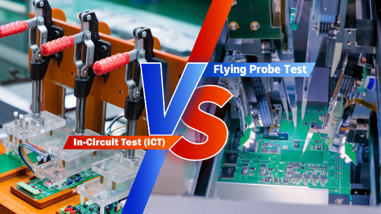
In today's rapidly evolving field of printed circuit board (PCB) assembly and testing, ensuring high product quality and reliability is crucial for PCB manufacturers and electronic designers. When searching for efficient, scalable, and cost-effective testing solutions, two approaches stand out: in-circuit testing (ICT), commonly known as "bed of nails" testing, and flying probe testing (FPT).
Both are considered among the best testing methods, but the choice between ICT and FPT remains an ongoing debate requiring deeper understanding and discussion. Selecting the appropriate testing method based on different production scales, design, and testing requirements is critical.
This guide is a comprehensive navigation tool to help you understand these two testing systems. It includes not only real-world examples and practical tips but also expert opinions. Through this guide, you will gain a comprehensive understanding of the key differences between them—flying probe testing vs. ICT, flying probe testing vs. in-circuit testing—the advantages of each test setup, and the scenarios where each testing method is best suited for your PCB testing needs.

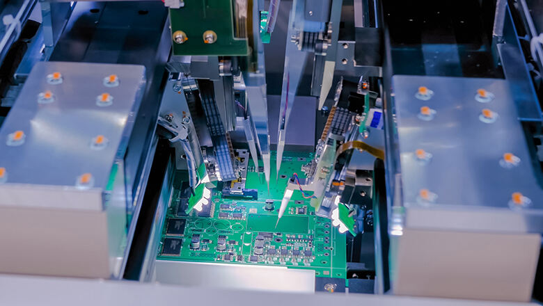
Flying probe testing is a highly flexible, tool-free testing solution suitable for PCB prototyping, small-to-medium volume production, and New Product Introduction (NPI) testing. It eliminates the need for dedicated pin positioning fixtures, instead using moving test probes (up to eight or more) controlled by advanced robotics and test software.
The key advantage of this testing method lies in its design, which combines speed and adaptability, allowing for physical contact with specific test points (pads, vias, components) on the PCB without the need for expensive and labor-intensive dedicated fixtures. This testing system is ideal for applications requiring frequent design adjustments and ensures easy updates when new versions are released.
Flight probe testing can include dynamic "test LED" checks, SMD component orientation checks, and (if configured correctly) dynamic IC programming.

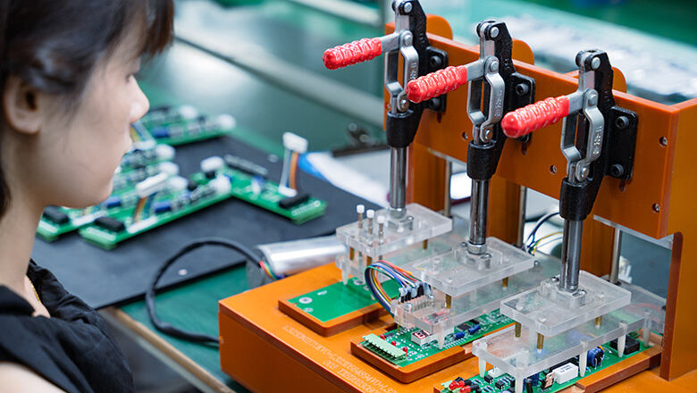
In-circuit testing (ICT), also known as bed of nails testing or simply ICT testing, has long been the industry standard for mass production. This method uses specialized testing equipment equipped with hundreds or even thousands of spring-loaded pins, each precisely aligned with a specific test point or node on the printed circuit board.
ICT testers (also known as in-circuit testers) can test all nodes on a printed circuit board simultaneously with a single press, enabling high-speed automated inspection of the entire board to detect open circuits, short circuits, digital errors, solder bridges, and other assembly defects.
Factor |
Flying Probe Test |
In-Circuit Test (ICT) |
Setup Cost |
Low (no fixture) |
High (fixture required) |
Test Cycle/Time |
Longer test cycle per PCB |
Extremely fast—high-volume production |
Volume Suitability |
Prototyping, low-volume, quick changes |
Large, stable production runs |
Test Coverage |
Flexible, can hit test points unreachable by bed of nails |
Maximum with full board access |
Change Management |
Easy, software-driven |
Expensive—new fixture for every major change |
Best Testing Method |
For design changes, DFT reviews, rapid feedback |
For stable layouts, efficiency, throughput |
Contact Method |
Movable probes make contact at each point |
Fixed pins (bed of nails fixture) touch all points at once |
Risk of Damage |
Very low |
Higher; risk with delicate pads |
Aspect |
ICT Test |
Flying Probe Test |
Fixture Type |
Dedicated test fixture with multiple fixed pins (bed of nails fixture) |
No dedicated fixture; uses movable flying probes |
Testing Process |
Simultaneous testing of all points |
Sequential testing; probes move from one test point to another |
Testing Time |
Seconds per PCB—ideal for high-volume |
Minutes per PCB—best for prototypes and lower-volume jobs |
Flexibility |
Low; each change needs new fixture |
High; software adaptation, rapid reprogramming |
Cost Per Test |
Low at high volume, but upfront fixture cost is high |
Higher per board, but virtually no upfront cost |
Test Coverage |
Best for open circuits, short circuits, value checks, and integrated function |
Excellent for open/shorts, some value checks, but may be limited for dense BGA or inner-layer faults |
Test Complexity |
Can perform functional tests with extra setup |
Limited functional testing; focus on electrical and component checks |
Best Use Case |
In-circuit testing for mature, high-volume boards |
Rapid prototyping, NPI, low-volume, and boards with frequent design changes |
Risk |
Pin wear, potential pad damage (especially if not maintained) |
Minimal risk, gentle on pads and circuit boards |


Why use hybrid testing? Combining successive flight testing and in-circuit testing can meet the diverse assembly testing needs of modern printed circuit board production lines, from design verification to mass production:
Q: Which test method is best for DFM/DFT validation?
A: Flying probe measurements offer unparalleled advantages for design iteration and manufacturing-oriented design efforts. They require no hardware installation and allow for rapid response to design changes.
Q: What is the main difference—flying probe vs in-circuit test?
A: ICT technology uses a bed of nails to test all nodes of a printed circuit board simultaneously, making it ideal for high-volume, low-cost applications. Moving probe testing, on the other hand, uses a sequential (moving probe) testing method, suitable for small-batch production and capable of flexibly handling multiple PCB modifications.
Q: Can flying probe test perform complete functional testing?
A: While feasible for simple circuits, ICT (along with functional devices) are often more commonly used to fully verify the operation of a circuit.
Q: What is the risk of relying only on one test system?
A: Relying on a single inspection method may lead to missed defects or bottlenecks during new product launches and mass production. Combining two inspection methods (or supplementing them with automated optical inspection or X-ray inspection) can meet all inspection coverage requirements.
Q: How fast is ICT vs flying probe?
A: ICT systems can typically test hundreds of printed circuit boards per hour. In contrast, Flying probe testing may only be able to test a few dozen per hour, depending on the complexity of the circuit board.
The choice between in-circuit testing and flying probe testing ultimately depends on production requirements, board complexity, budget, and time-to-market. Flying probe testing excels in the early, rapid, and innovative stages of product development, enabling rapid design iteration and immediate feedback. In-circuit testing, with its dedicated equipment and simultaneous testing capabilities, provides comprehensive, rapid, and cost-effective test coverage for mature, stable, and large-scale assembly lines.