All Categories
News
Home> News

Blind and Buried Vias in PCB Design: A Manufacturer's Guide

2025-11-10

Introduction to Blind and Buried Vias

In the fast-paced world of electronics, With the market's demand for high-tech hardware products,the need for miniaturization, higher performance, and more complex functions on smaller circuit boards has never been greater. Designers and PCB manufacturers been have also faced new challenges,than they strive to pack as much functionality as possible into every square millimeter. This challenge has led to the use of blind and buried vias in HDI PCBs and multilayer PCB designs. These hidden vias allow unprecedented space optimization, denser circuit layouts, and advanced signal integrity.As an experienced circuit board manufacturer, LHD TECH has seen its processing and manufacturing capabilities evolve along with the updates of market products over the past 20 years. From the optimization of the system to the precise manufacturing capability of the equipment, and then to the efficient management of the production team, all keep pace with the demands of The Times.

Let's return to the topic technology itself, But what exactly are these vias in PCB design? How are blind vias and buried vias created, Compared with the traditional through-hole process, in which sectors is it stronger and whose audience is it? In this comprehensive guide, We will delve into technology and unravel the mysteries of blind and buried vias, explore how they’re used by experienced PCB manufacturers, and show how they offer powerful advantages for your next complex PCB design.

The Role of Vias in PCB Design

Let's first take a look at the via process in PCBS, From the perspective of fundamental principles vias in PCB are the electrical connections that bind different PCB layers together. Every multilayer PCB—from simple 4-layer boards to complex 30+ layer stacks—relies on vias to shuttle signals, power, and ground between the outer layer of the PCB and the inner layers of the PCB.

Why are vias used?

  • Vias connect an outer layer to inner layers for flexible routing.
  • Vias are plated with copper, making an electrically conductive path between layers of a PCB.
  • Vias are commonly used to reduce signal path length, improve signal integrity, and optimize board space.
  • The use of blind vias and buried vias allows engineers to dramatically reduce the PCB’s overall size and the number of through-hole vias needed.

Based on the above understanding in modern HDI and multi-layer PCB circuits, vias are pressed together in carefully planned stack-ups to balance performance, reliability, and manufacturability.

The Fundamentals: Types of Vias in PCB

How many types of Vias are there that we commonly see?How to understanding the different types of vias is fundamental to mastering PCB design and achieving optimal board performance.

This table makes a clear distinction:

Via Type

Layer Connections

Use Case

Visibility

Complexity

Through-Hole Vias

Outer layer to opposite outer layer

General multilayer signal routing

Both surfaces

Low

Blind Vias

Outer layer to inner layers

HDI, BGA breakout, SMT boards

One surface

Moderate

Buried Vias

Internal layers only

Power/ground isolation, dense PCBs

Not visible

High

Micro Vias

Adjacent layers, extremely small

Ultra-dense designs, HDI PCBs

May be hidden

Very High

What are Blind Vias?

blind-via​.jpg

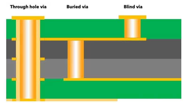
Today, we are discussing blind holes and buried holes. So, what exactly is the structure and principle of blind holes. A blind via is a via that connects an outer layer of a PCB to one or more inner layers, without passing through to the opposite outer layer. It is “blind” because it is only visible and accessible from one surface,So blind vias are often used to reduce the number of layers on a PCB.

Key Details & Benefits

  • Blind vias connect the top or bottom surface to selected inner layers, this is to achieve the optimal utilization of the available routing layers.
  • Blind vias do not penetrate the entire PCB thickness, not only save valuable space on the PCB and freeing up opposite surfaces for other traces or components.
  • Because blind vias are drilled only partially through the board, they allow for denser circuit layout and are typically used in HDI PCBs and BGA breakout patterns,it has greatly improved the utilization rate of wiring.
  • Blind vias are typically small (less than 0.15 mm in diameter) and there are extremely high requirements for drilling machinery and equipment,so must be require precision laser or more precise mechanical drilling.
  • Use of blind vias can reduce PCB thickness and its purpose is help achieve high component density for modern products.

How Blind Vias Are Drilled and Made

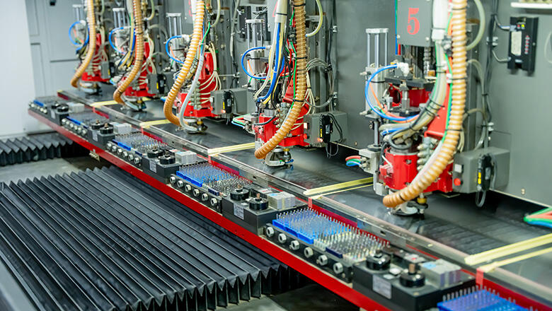
Blind vias are drilled during specific lamination and drilling steps. Their quantity and position and depth must be controlled to avoid breaking through unintended layers. They are then plated with copper to form conductive paths. Creating blind vias involves careful preparation to prevent air trapped in the PCB or incomplete plating, ensuring robust reliability.
What are Buried Vias?

buried-vias.jpg

Unlike blind holes, buried holes do not penetrate the outer layer of the plate.A buried via is a via that connects two or more inner layers of a PCB, and is not visible or accessible from either outer layer. These are also called hidden vias, as they’re “buried” between the PCB’s surface layers.Let's learn more about buried holes together.

Key Details & Benefits

  • In the process of manufacturing buried vias are drilled and plated during the manufacturing of inner sub-assemblies, before the outer layers are laminated.
  • From the perspective of the structure of multi-layer boards buried via connects two inner layers—for example, layers 3 and 4 in an 8-layer PCB—providing routing options without using surface real estate.
  • The difference is buried vias in PCB design allow designers to isolate signal paths, ground, or power distribution, but it greatly benefiting complex or mixed-signal designs.
  • Because buried vias are not visible after final lamination, It is a major advantage what they can maximize PCB layer utilization and reduce crosstalk.
  • Buried vias are typically used in advanced multilayer PCBs for telecommunications, aerospace, and high-density electronics.

Other Types of Vias in PCB

Through-Hole Vias

In printed circuit boards, Through-hole is a hole structure that connects circuits between different layers of the PCB. Through-holes allow electrical signals to be transmitted between board layers and are one of the most fundamental and common types of holes in traditional PCB design.It has the following characteristics:

  • Connect the entire PCB stack, from top to bottom.
  • Used for standard multilayer PCBs, component leads, and connectors.
  • Consume more space and can limit high-density routing.

Micro Vias

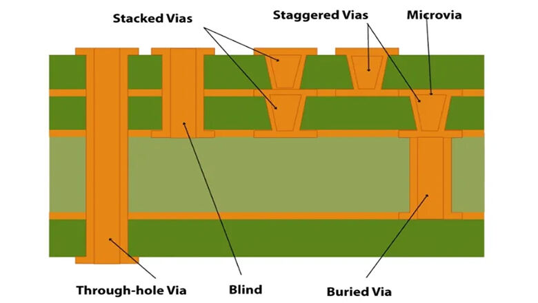
Microvia refers to a through-hole with a very small diameter, typically 0.1mm or smaller, and is often used in different design layers of high-density interconnect (HDI) printed circuit boards. It has the following characteristics:

  • Extremely small vias connecting only adjacent layers, formed using laser ablation for HDI PCB.
  • Can be stacked or staggered, and are often used in dense smartphone, wearables, or medical device designs.
  • Require advanced production and inspection by experienced PCB manufacturers.

Comparison Table: Blind vs. Buried vs. Through-Hole Vias

Feature

Blind Via

Buried Via

Through-Hole Via

Visibility

Visible one surface

Not visible (hidden vias)

Visible both surfaces

Connection

Outer to one/more inner layers (not full stack)

Inner-to-inner layers only

Top to bottom (all layers)

Space Saving

High

Very High

Low

Cost

Moderate

High

Low

Why Use Blind and Buried Vias? Benefits and Limitations

blind-via-pcb​.jpg

In this chapter, we focus on blind holes and buried holes. In the design considerations of product requirements, When we using blind vias and buried vias what advantages and limitations do they have? Let's make a summary and distinction together.
Advantages of Blind and Buried Vias

  • Space Optimization: Compared with the through-hole design it reduce the PCB size and thickness, allowing more components and traces in less space.
  • Signal Isolation: It can not only isolate critical signals or power planes, but also shielding them from EMI/Crosstalk.
  • Enhanced Routing: Vias connect outer and inner PCB layers for more flexible, efficient layouts.
  • Complex PCB Design: Make it feasible to use dense BGAs, FPGAs, and fine-pch pitch ICs without dramatically increasing the number of PCB layers or the board’s footprint.
  • PCB Layer Utilization: Buried vias provide connections within inner layers of a PCB without consuming outer layer real estate, reducing congestion and enabling layered signal or power plane separation.It has especially contributed to technological breakthroughs in the aviation/communication/medical equipment industries.
  • Improved Signal Integrity: Using blind and buried vias in PCB design reduces the formation of signal stubs, minimizing reflections, loss, and electromagnetic interference, which is vital for high-speed and RF circuits.
  • Thermal Optimization: Effective via placement can help distribute and dissipate heat, mitigating the risk of hot spots and improving long-term reliability in complex PCB assemblies.

Limitations of Blind and Buried Vias

  • Increased Manufacturing Complexity: The manufacturing of blind and buried vias involves additional drilling and lamination steps, only feasible with experienced PCB manufacturers and precise quality control,and test the manufacturer's production capacity.
  • Greater Production Cost: Each extra lamination cycle, filling step, or additional via means increased PCB production cost and material use—especially in multi-layer PCB and HDI PCB products.So the price of pcb products is also relatively high.
  • Testing and Inspection: Blind and buried vias are sometimes difficult to inspect for defects, requiring advanced techniques like X-ray imaging to ensure quality.
  • Potential Reliability Risks: If process control isn’t perfect, risks like air trapped in the PCB, incomplete copper plating, or delamination can occur.

Manufacturing Process: Creating Blind and Buried Vias

blind-vias​.jpg

Overview

The pcb manufacturing process of blind vias and buried vias on PCBS is complex and precise. However, the manufacturing process of these vias is of great significance in enhancing the performance of PCBS, reducing the number of board layers, and increasing space utilization.

  1. Stack-Up Design: The laminated design is the structural basis of blind buried holes.The design begins by mapping the layers of a PCB and where vias need to connect—blind via connects an outer layer to one or more inner layers; buried via connects two inner layers but not extending to the surfaces.
  2. Drilling:
  • Blind vias are drilled only partially through the stack (outer to inner), typically using highly precise mechanical or laser drilling.
  • Production of buried vias requires drilling in sub-assembled layers before full stack lamination it unlike blind holes.

3.Lamination: The lamination treatments of the two are also different.For buried vias, layers are pressed together, and more layers are subsequently added. Blind and buried via PCB fabrication requires perfect registration and alignment.

4.Plating: All vias, including through-hole, blind and buried via, are plated with copper using chemical and electroplating to guarantee conductivity.

5.Testing: Advanced testing—especially for buried vias in PCB—such as X-ray or micro-section analysis ensures vias are correctly formed and reliable.

Applications and Use Cases

Blind and buried vias have become standard in advanced PCB design。 It can significantly improve the space utilization rate, reduce the board area, lower the number of floors, and make the design more compact ,and it across virtually every industry area where high performance, density, or size reduction is needed.

Examples of Industries Using Blind and Buried Vias

  • HDI PCB for Smartphones: Blind vias connect outer pads to internal routing, and while buried vias in PCB minimize EMI and route critical high-speed signals with precision,the market demand for smart phones is increasing widely.
  • Networking Equipment: Buried via connects two isolated planes in a multi-layer PCB for signal integrity in telecommunications switches and routers.
  • Medical Wearables: Blind and buried vias provide signal isolation in tiny, highly reliable implantable devices,it provides a vast space for optimization and assistance for current medical equipment.
  • Automotive Electronics: In the market environment of a comprehensive upgrade in the automotive manufacturing industry,ADAS and infotainment modules use both blind and buried vias to shrink board size, ensuring performance in rugged environmental conditions.
  • Aerospace Applications: Buried vias provide robust shielded transmission for sensor or control data, with superb reliability even under vibration or temperature extremes.

Cost Factors and Reliability
Cost Factors

Due to the fact that blind buried hole technology requires special processes such as drilling, copper plating, and coating treatment, it usually increases production costs. Especially in mid-to-low-end products, it may be difficult to use this technology. Therefore, the cost increase is an important factor in the process requirements of some industries.

  • Advanced Manufacturing Steps: The use of blind via and buried via requires more production stages than traditional through-hole vias, raising both setup and per-board expenses.
  • Material Choices and Layer Count: The more layers of a PCB, the more frequent the manufacturing of blind and buried vias is required. High-Tg pre-pregs and specialty foils further increase costs.
  • Testing and Inspection Costs: Inspection for hidden vias—especially buried hole structures—often incorporates extra X-ray/CT or destructive microsectioning.

Reliability Considerations

Despite the rising costs, some technological hardware products in certain fields have high requirements for the heat dissipation effect and mechanical strength of control boards. The selection of blind buried hole manufacturing requirements is also an inevitable path for product iteration.

  • Proper Plating and Filling: Ensuring vias are plated with copper evenly and, if necessary, filled, is crucial for electrical reliability and for preventing solder/thermal failure.
  • Thermal Cycling Stress: Vias, especially hidden vias, are vulnerable to cracking or delamination if not built with the right process and materials.
  • Air Trapped in the PCB: Defects from air or voids can lead to early field failures.
  • Engage Experienced PCB Manufacturers: Rely on partners who understand how to correctly fabricate, inspect, and test blind and buried via PCB designs for long service life.

Design Tips for Using Blind and Buried Vias

The production requirements for blind buried holes are so high and their functions so significant that there are also high demands on the design structure. From the customer's understanding of product needs, to the selection of materials, and then to the cost and the manufacturing capacity of the supplier, a reasonable design should be made by comprehensively considering all these factors.The following factors should be given priority consideration:

  • Early Consultation with PCB Manufacturers: Use experienced PCB manufacturers and check their technical restrictions on blind via depth, aspect ratio, and minimum drill size.
  • Stack-Up Planning: When designing a multi-layer PCB, clearly delineate which signals or power must stay isolated and where buried vias are added for best layer utilization.
  • Avoid Overuse: Only use blind vias and buried vias where essential. Overuse increases costs and decreases yield.
  • Via Filling: For via-in-pad and microvias, always specify if the via should be filled or capped.
  • Thermal Relief: Connect power/ground vias to planes using “thermal relief” pad designs, providing better solderability and reducing stress risks.
  • Test Coupons: Ask for coupons to enable destructive sectioning during production of buried vias to confirm manufacturing quality.
  • Address Stacked and Staggered Vias: When necessary, stagger microvias or limit the stack-up of blind and buried via groups for improved reliability.

Frequently Asked Questions

Q: How do blind and buried vias differ from standard through-hole vias?
A: Blind vias connect an outer layer to one or more inner layers, but not completely through the board. Buried vias connect two inner layers, “hidden” after lamination. Through-hole vias connect surface to surface straight through the PCB.
Q: When should I use blind and buried vias in pcb manufacturing?
A: Use blind and buried vias for dense HDI pcb layouts, fine-pitch BGAs, high-speed signals, or when minimizing board size is essential.
Q: Are blind and buried vias reliable?
A: Yes, with experienced PCB manufacturer partners and correct process controls for drilling, plating, and filling. Challenges exist in ensuring every via is correctly formed and inspected.
Q: Can I mix via types in one board?
A: Absolutely! Most modern complex PCB designs use a combination of traditional through-hole vias, blind vias, buried vias, and even microvias depending on circuit need.
Q: How does the production of buried vias impact lead time?
A: Adding buried vias to a PCB increases lead time due to extra lamination, additional drilling, and more thorough inspection. Plan accordingly.

Conclusion: Should You Use Blind and Buried Vias?

If you're working on a tight, complex, or high-tech PCB design, these special vias are pretty much essential. They help shrink your board size, keep your signals clean, and make routing all those complicated connections possible in today's gadgets.But here's the catch – they do cost more to make, and you'll need a manufacturer who really knows their stuff. That's why it's smart to loop in your fabrication partner early, only useblind and buried vias where you really need them, and double-check they can handle your design before sending over your files.
Bottom line: if you're dealing with HDI PCBs, trying to cut down on regular through-holes, or aiming for killer performance in a multilayer PCB, you really shouldn't overlook what blind and buried vias can do for you.

blind and buried vias in pcb design a manufacturers guide-0

Get a Free Quote

Our representative will contact you soon.
Email
Name
Company Name
Message
0/1000