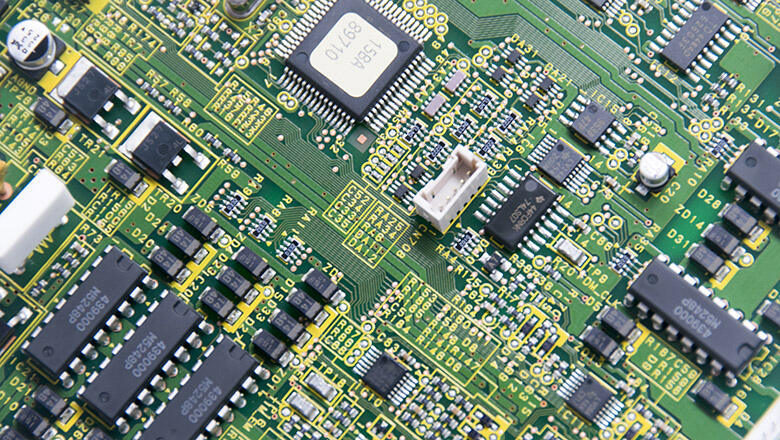
Introduction to IC Package Technology

Integrated circuits (ICs) form the foundation of all modern electronic systems. Their packaging technology provides a crucial interface between silicon chips and the external environment, and enable large-scale applications, miniaturization and high-reliability operation. This guide traces the development history of integrated circuit packaging technology, from the initial major breakthroughs to the current cutting-edge solutions.
A good chip packaging must not only protect the chip but also meet requirements such as stable electrical performance, efficient heat dissipation, simple manufacturing processes, and high durability. From traditional DIP packaging to innovative technologies such as 3D packaging and FOWLP, packaging technology is constantly evolving.
IC Package Fundamentals
What is an IC Package? Why is It Important?

An integrated circuit (IC) package is a protective enclosure used to securely mount and interconnect chips (or, in the case of multi-chip modules and advanced packaging) in an electronic system. Its main functions include:
- Protection: Protects integrated circuit chips from moisture, impact, contamination, and electrostatic discharge.
- Electrical Connection: Chips are connected to larger systems via metal wires, solder balls, or pads, enabling powerful signal transmission.
- Thermal Management: It helps dissipate the heat generated by integrated circuits onto the printed circuit board or in the environment, thereby ensuring reliable and continuous operation. Improving heat dissipation is crucial for high-power and high-frequency circuits.
- Identification: This document contains all the information required for assembly, operation, and maintenance, as well as compliance with legal and regulatory requirements.
The Scope of this Comprehensive Guide
This guide to IC package selection and design answers:
- What are the common IC package types?
- In terms of electronics, thermodynamics, mechanics and manufacturing—what’s the same and what’s different between different kinds of IC packages?
- As semiconductor technology keeps developing, how has IC packaging technology changed?
- How important is new innovative packaging tech for AI, 5G and the Internet of Things?
- Which packaging solution best suits your application requirements?
In word, this is a comprehensive and important guide. It aims to help readers understand integrated circuit types, choose appropriate packages, and understand global trends in packaging technology.
The Building Blocks of IC Packages
Basic Package Components
Regardless of the package type, all integrated circuit packages share a few basic components, which are combined to produce high-performance, reliable electronic products:
- IC Die (Chip): Hearts are typically made using advanced semiconductor manufacturing technology, with silicon as the primary material.
- Package Substrate: It can securely connect chips (using wire bonding or flip-chip technology) and provide a platform for transmitting signals between the chip and external pins or solder balls.
- Leads, Balls, or Pads: These pins are located on the side, bottom, or all four sides of the package and are used to connect to the PCB.
- Encapsulation or Sealing Material: Plastic or ceramic materials used for machinery and environmental protection.
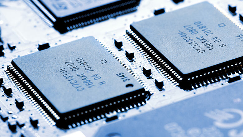
- Markings: Identify markings, batch numbers, direction markings, and possible anti-counterfeiting features.
- Thermal Enhancement Features: Exposed thermal pads, heat sinks, and heat plates can improve thermal management.
IC Package Materials and Mechanical Properties

Materials for IC Packaging
As packaging technology becomes increasingly complex, the selection of packaging materials becomes more and more important.
- Plastic/Epoxy: It is affordable and suitable for most commercial applications, but its performance is limited in high temperature and high humidity environments.
- Ceramic: They have excellent reliability and are suitable for high-power, military and aerospace applications, especially for withstanding high thermal and mechanical stresses.
- Metal/Composite: Heat sinks and lead frames are increasingly being used in power semiconductors and high-frequency applications.
Packaging Materials Table:
Package Type |
Typical Materials |
Use Case |
Key Benefit |
Plastic/Epoxy |
Epoxy resins, plastics |
Consumer, SMD, DIP |
Cost, easy to mass-produce |
Ceramic |
Al2O3, SiN, etc. |
Military, auto, power |
Advanced thermal, reliability |
Composite, Metal Base |
Copper alloys, alloys |
Power, high freq. |
Heat spreading, performance |
Mechanical Properties and Package Features
- Vibration/Shock Resistance: It is crucial for the automotive, aerospace, and industrial electronics industries.
- Moisture Sensitivity: Based on the MSL (Moisture Sensitivity Level), plastic packaging requires careful storage/handling.
- Package Dimensions: This will affect PCB layout, stacking height in 3D IC applications, and device thickness in mobile devices.
- Surface Mount Capability: By directly attaching components to the PCB, this packaging method enables more efficient automated assembly.
IC Package Types, Sizes, and Classifications

To support the explosive growth of applications in fields such as the Internet of Things, high-performance computing, automobiles, and wearable devices, various packaging types have emerged.
Through-Hole Technology
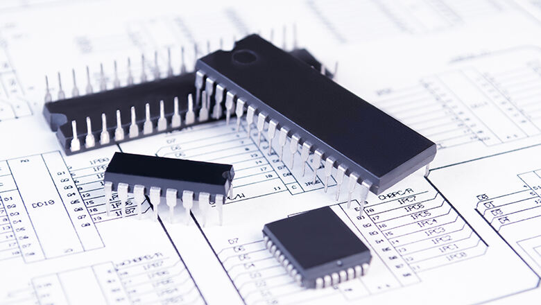
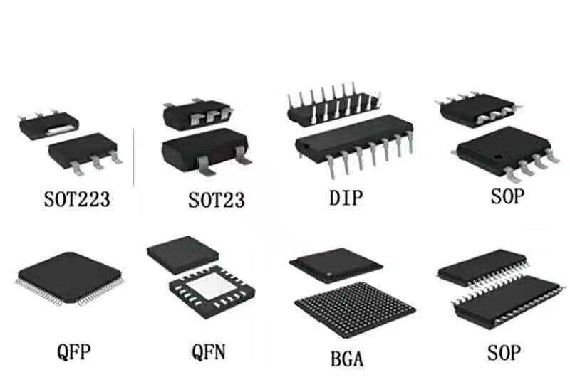
- Dual In-line Package (DIP): The earliest integrated circuit package. These parts are small, reliable, and easy to connect or replace. You can still find them in prototypes, power systems and older products.
- TO-92, TO-220: This type of package is commonly used for small-signal transistors (TO-92) and power devices (TO-220), allowing for secure mounting and easy connection to heat sinks.
Surface-Mount Technology (SMT) and Surface Mounted Packages
- Small-Outline Package (SOP), SOIC: Surface mount open (SOP) packages are widely used in consumer electronics and automotive electronics. SOP package are thinner than SOIC package, thus enabling higher PCB wiring density.
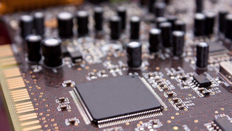
- Quad Flat Package (QFP): This package has pins on all four sides, making it suitable for microcontrollers and field-programmable gate arrays (FPGAs) with a large number of pins.
- Quad Flat No-Lead (QFN): The pins do not extend beyond the package body; the pads are located at the bottom of the package. The main advantages about this design is it works great for heat dissipation and uses space efficiently.
- Small-Outline Transistor (SOT): The small transistors/diodes used in surface mount technology have a high density.
Array and Advanced IC Packaging Technologies
- Ball Grid Array (BGA): The solder balls beneath the chip are arranged in a grid pattern. This design has an interconnect density of hundreds to thousands, so it’s perfect for CPUs, FPGAs, and high-speed memory.
- Land Grid Array (LGA): Similar to BGA, but with gold-plated pads—ideal for server CPUs, offering high reliability and high density.
- Chip Scale Packaging (CSP): Almost as small as the chip itself—ideal for smartphones, medical devices, and the Internet of Things.
- Wafer-Level Packaging (WLP): These packages are formed directly at the wafer level, enabling ultra-small, high-performance, low-profile solutions.
Special Advanced Packages (continued)
- System-in-Package (SiP): Multiple chips and passive/active components are integrated into a single package. These chips fit wearable devices, micro-radios, advanced ICs, and IoT nodes. They maximize space use and put multiple functions into one package.
- 3D IC / 3D IC Packaging / 3D Packaging: Stacked chip structures (utilizing through-silicon vias and wafer bonding technologies) enable high-bandwidth chip-to-chip communication and unparalleled integration. 3D ICs are a hallmark of cutting-edge AI processors and high-end mobile SoCs.
Types of IC Packages and Applications
IC Package Type |
Assembly Process |
Typical Application |
Package Features |
DIP (Through-Hole) |
Soldered, socketed |
Legacy, prototyping, analog |
Large, easy to handle |
SOIC/SOP (SMD) |
Surface-mount |
Consumer, automotive |
Compact, cost-effective |
QFP/QFN (SMD) |
Surface-mount |
MCUs, FPGAs, wireless, SMC |
High pin-count/density |
BGA |
Surface-mount (reflow) |
CPUs, GPUs, memory |
High I/O, improved thermal |
CSP/WLP |
Wafer-level, SMD |
Mobile, sensors, IoT |
Ultra-compact, low profile |
SiP/3D IC |
Custom/advanced process |
Wearables, servers, high-perf AI |
Multi-die, advanced perf. |
Information Contained in an IC Package

The information laser-marked or engraved on each integrated circuit package is very important, as it affects not only assembly but also system performance.
- Part Number and Package Type: For identification, procurement, and quality control.
- Package Dimensions/Outline: Specifies the size, lead pitch, and placement for design and pad layout.
- Pin Configuration: The arrangement of pins, pads, or balls and the signals or forces they represent.
- Material/Environmental Details: It is RoHS compliant and lead-free, featuring protection against moisture and chemicals.
- Lot Codes and Date Codes: Traceability for quality and warranty tracking.
- Orientation and Assembly Marks: Notches, dots, chamfers, or laser markings indicate pin 1 and the correct orientation.
- Thermal Ratings: Maximum junction temperature, power dissipation, and guidelines for improved thermal performance.
Packaging design is governed by rigorous standards, guaranteeing reliability, interoperability, and manufacturability.
- IPC-7351: Define standard pad patterns for surface mount device packages to ensure package consistency in PCB design and automated assembly.
- ANSI Y32.2-1975: Defines schematic symbols for all types of IC packages.
- ISO 10303-21: The STEP format is essential for exchanging 3D models of packaging outlines and dimensions between design tools.
- JEDEC and SEMI Standardization: Especially for multi-source semiconductor packages, thermal ratings, humidity sensitivity, testability, and package compatibility are very important.
- RoHS/REACH Compliance: Ensure that integrated circuit packaging materials meet global environmental standards.
Rules and Best Practices for IC Package Design

The packaging of an integrated circuit must take into account a range of electrical, thermal, and mechanical requirements,including:
- Follow IPC and JEDEC footprint guidelines: Pad patterns optimized for surface-mount packaging.
- Optimize Thermal Paths: Use exposed pads, thermal vias, and sufficient copper layer beneath the thermal package.
- Check Pad and Pin Pitch: Choose a package pitch that suits the precision of your assembly process. Fine-pitch BGAs or QFNs may require X-ray inspection and could increase assembly costs.
- Utilize Clear Orientation Marks: Pin 1 is clearly marked on the package and aligned with the PCB silkscreen to prevent assembly errors.
- Design for Manufacturability: Avoid using too many package types on the same PCB, and choose standard, mass-produced packages whenever possible to ensure optimal packaging costs and supply chain stability.
- Leverage Simulation Tools: The latest electronic design automation (EDA) kits can simulate signal integrity, mechanical stress, and thermal performance, making advanced package selection and integration more reliable.
How to Choose the Right IC Package
Consider the following factors when selecting a package or package type:
- Performance Requirements: For high-speed, low-noise, or high-power-density applications, BGA or 3D IC packages are more suitable. SOIC or QFN packages offer a cost-effective solution for many medium-power applications.
- Thermal Considerations: CPUs and power ICs require better heat dissipation—look for packages with heat sinks, thermal pads, or advanced substrate technology.
- Mechanical and Environmental Needs: When factors such as vibration, shock, or moisture need to be considered (e.g., in automotive or industrial control applications), advanced ceramic or metal packages can provide maximum protection.
- Manufacturability and Assembly: SMT packaging offers the highest throughput for automated assembly; through-hole packaging may be suitable for prototyping and certain applications with high reliability requirements.
- Package Size and PCB Constraints: For ultra-compact form factors (portable devices, hearing aids), use CSP, QFN, or WLP; for breadboard compatible or traditional products, use DIP or SOIC.
- Cost and Supply Chain: Standard packaging solutions can typically reduce packaging costs and shorten delivery times. When designing for mass production, we focus on choosing common, already-made package types. This makes it easy to get the parts and keep costs under control.
Challenges and Limitations in IC Packaging
Even though semiconductor packaging tech has improved a lot, some ongoing challenges still need attention:
- Thermal Dissipation: As chip power consumption continues to increase, the reliable heat dissipation capabilities of traditional packages are nearing their limits. With new developments like FOWLP and built-in thermal paths, selecting a package is still very important, especially for heat-heavy SoCs.
- Miniaturization Limits: As package size decreases, the difficulty of assembling, deforming, and inspecting fine structures increases (especially for BGA and WLP), thereby increasing the risk of costly failures in the field.
- Signal Integrity at High Frequencies: Higher data transmission rates mean that signal loss, crosstalk, and electromagnetic interference are more difficult to control inside the package.While advanced substrate and shielding designs improve performance, they also increase packaging costs.
- Mechanical Reliability: Packaging must be able to withstand shocks, vibrations, and repeated temperature changes, especially in harsh conditions such as those experienced by automobiles and industrial electronics.
- Environmental and Regulatory Compliance: Faced with increasingly stringent regulations, manufacturers must ensure that packaging materials are non-toxic, recyclable, and compliant with global RoHS/REACH/environmental standards.
- Complex Assembly Process: In advanced packaging processes (SiP, 3D IC, FOWLP), assembly processes can include chip stacking, wafer-level manufacturing, and complex wire bonding or flip-chip technologies.
Future Trends in IC Package Technology
Packaging Innovations On the Horizon
- Fan-out Wafer-Level Packaging (FOWLP): Advanced circuit packaging integration processes involve placing the chip on a substrate, packaging it, and then redistributing the chip using fine wiring—achieving high I/O performance and heat dissipation in a thin and scalable form.
- 3D Packaging and Chiplets: True 3D IC stacking, chip-based system integration, and advanced packaging types with vertical/horizontal interconnects define the next era of performance scalability and functionality in a single package.
- Biodegradable Materials: To minimize e-waste, packaging materials for integrated circuits, such as compostable plastics and non-toxic encapsulation materials, are being researched and have already been used in some disposable consumer products.
- Smart Packages: The combination of health sensors, active cooling (microfluidics/Peltier effect), and self-monitoring of pressure and temperature is advantageous for critical applications.
- AI-Driven Package Design: AI can now accelerate the automatic optimization of package type, pin assignment, and substrate structure, thereby simultaneously improving electrical, thermal, and cost performance.
Frequently Asked Questions (FAQs) About IC Package Technology
Q: What are the most common IC package types today?
A: SOP, QFP, QFN, BGA, CSP, and WLP have become common packaging types in modern electronic products. However, through-hole packages (DIP, TO-220) are still used in some special applications and prototype products.
Q: What’s the difference between surface-mount packages and through-hole technology?
A: Surface mount devices are specifically designed for automated assembly directly on the surface of printed circuit boards, featuring smaller package sizes, higher circuit densities, and more reliable high-speed operation. In contrast, through-hole mounting technology requires the pins to be inserted into pre-drilled holes on the PCB, which can form a solid mechanical connection but requires more board space. When surface mounting has become the industry standard for modern mass production, through-hole technology is still indispensable in prototype verification, power electronics, and applications requiring high mechanical strength.
Q: What innovative packaging techniques are now being used in advanced ICs?
A: Advanced integrated circuit packaging technologies include 3D IC packaging, fan-out wafer-level packaging, system-in packaging, chip-level packaging, as well as modern wire bonding and flip-chip bonding technologies. These methods can effectively enhance electrical performance, achieve high pin density, and significantly optimize heat dissipation efficiency - which is crucial for high-power or high-frequency integrated circuit applications.
Q: How has IC packaging evolved to support the needs of high-speed circuits and AI?
A: With the advent of data centers, AI accelerators, and 5G, integrated circuit packaging technology must continuously evolve to minimize parasitic effects and improve thermal performance. Packaging solutions such as BGA, advanced substrates, thermally conductive vias, 3D packaging, and embedded passive components have become indispensable. 3D integrated circuits and chip architectures enable the tight integration of multiple functional components into a single package, thereby significantly improving computing density and energy efficiency.
Q: Which packaging materials are best for high-reliability or harsh environments?
A: Ceramic and metal packaging offer outstanding mechanical strength, thermal conductivity, and environmental resistance, it makes them ideal choices for applications in the automotive, military, and aerospace industries. For consumer electronics and general-purpose electronic products, plastic and composite packaging with good sealing properties typically achieve the best balance between cost-effectiveness and durability.
Q: How do I select the right package for my application?
A: When selecting an integrated circuit package type, electrical characteristics, power consumption, package size limitations, available manufacturing processes, and end-user reliability requirements should be considered. Equally important are the stability of the supply chain, total cost of ownership (including assembly and inspection), and relevant certifications (RoHS, JEDEC, and IPC compliance). This comprehensive guide to integrated circuit package selection will provide step-by-step guidance!
Conclusion
Due to the increasing demand for miniaturization, high speed, high energy efficiency and high reliability in electronics, integrated circuit packaging technology is undergoing unprecedented development. Modern packaging technology, as a crucial bridge between precise silicon chips and robust interconnected devices, is supporting innovative applications in a wide range of fields, from smart wearable devices to autonomous vehicles. As you can see in this comprehensive guide to integrated circuit packaging technology, choosing the right packaging solution is not a secondary consideration but a core key that determines the success or failure of any integrated circuit or electronic component.
