thick copper pcb
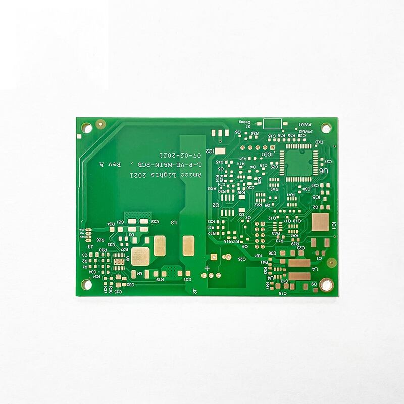
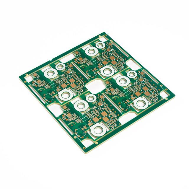
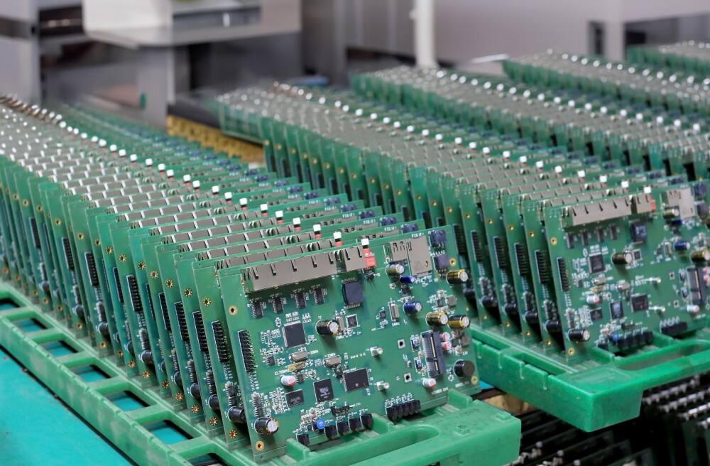
Thick copper PCB technology represents a significant advancement in printed circuit board manufacturing, characterized by copper layers that exceed standard thicknesses of 3 oz/ft². These specialized boards are engineered to handle high current capacities and enhanced thermal management requirements. The copper thickness typically ranges from 4 oz/ft² to 20 oz/ft², with some applications utilizing even thicker layers up to 200 oz/ft². These boards excel in applications demanding superior current carrying capabilities and heat dissipation properties. The manufacturing process involves precise control of copper plating and etching techniques to achieve consistent thick copper layers while maintaining tight dimensional tolerances. The technology incorporates advanced design considerations to address challenges such as impedance control, trace spacing, and thermal expansion. Thick copper PCBs find extensive use in power electronics, LED lighting systems, automotive applications, and industrial control equipment. They provide robust thermal management solutions through enhanced heat spreading capabilities and reduced thermal resistance. The boards can be manufactured in various configurations, including single-sided, double-sided, and multilayer designs, offering flexibility in application-specific requirements. Modern thick copper PCBs often integrate advanced materials and manufacturing techniques to optimize performance and reliability in demanding operating conditions.