High Density Interconnect (HDI) PCB Technology: Advanced Solutions for Modern Electronics

All Categories

hdi pcb

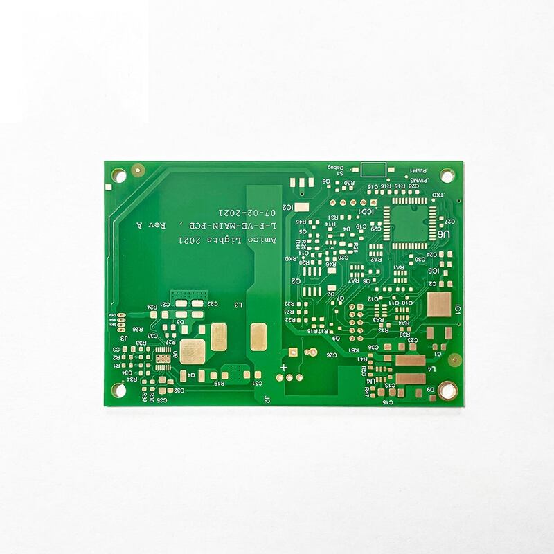
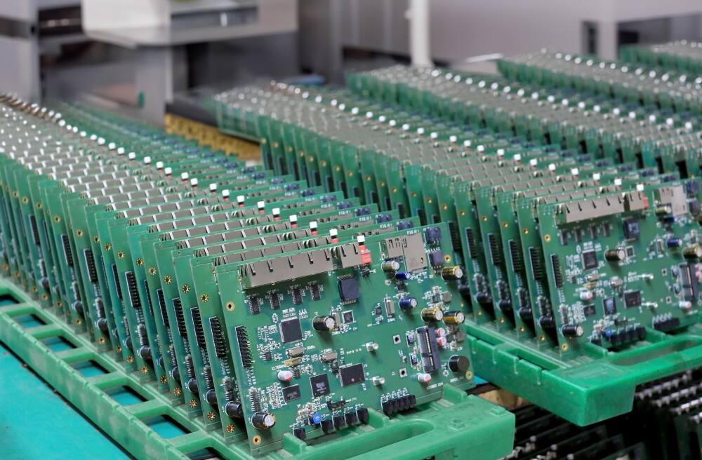
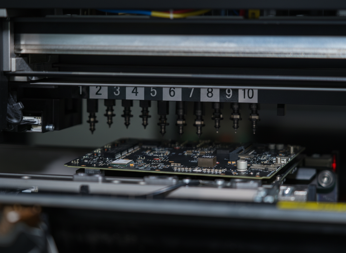
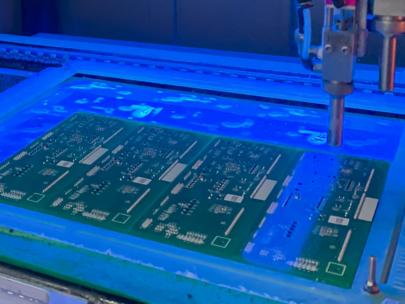
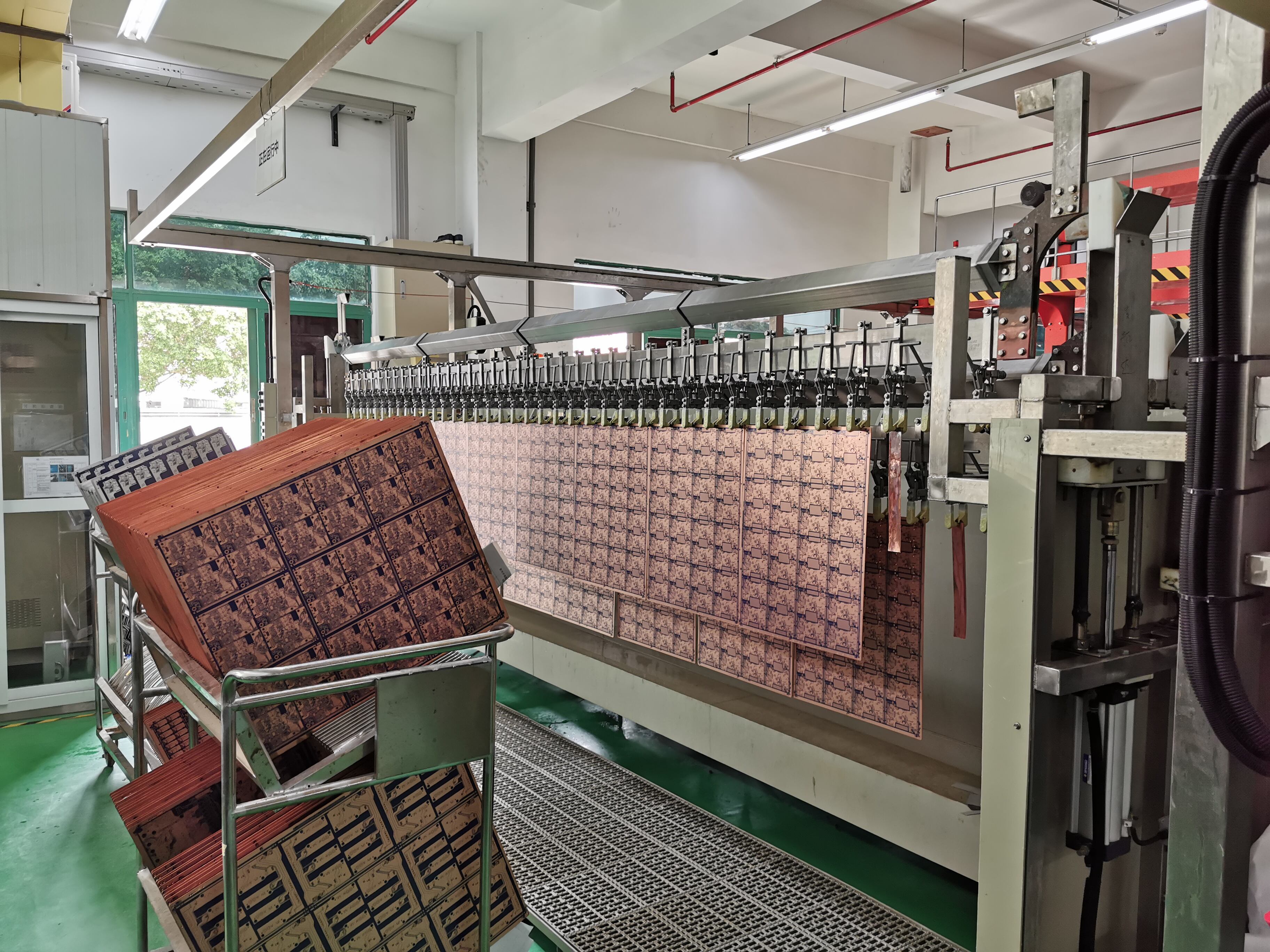
High Density Interconnect (HDI) PCB technology represents a significant advancement in printed circuit board manufacturing, offering enhanced capabilities for modern electronic devices. These sophisticated boards feature higher circuitry density and significantly more complex interconnections compared to traditional PCBs. HDI PCBs utilize microvias, blind and buried vias, and advanced lamination techniques to achieve superior connectivity in a compact form factor. The technology enables the creation of boards with finer lines and spaces, smaller vias, and higher connection pad density, making it possible to accommodate more components in a smaller area. HDI PCBs typically incorporate multiple layers, often ranging from 4 to 12 or more, interconnected through sophisticated via structures. The manufacturing process involves advanced techniques such as laser drilling, sequential lamination, and precise registration methods. These boards are particularly crucial in modern electronics where miniaturization and high performance are essential requirements. They find extensive applications in smartphones, tablets, wearable devices, medical equipment, aerospace technology, and other high-end electronic products where space optimization and signal integrity are paramount considerations.

New Products

HDI PCB technology offers numerous compelling advantages that make it an ideal choice for modern electronic applications. First, the reduced form factor allows for significant space savings while maintaining or improving functionality, enabling the creation of smaller and lighter electronic devices. The higher wiring density and more efficient routing capabilities result in shorter signal paths, which improve electrical performance and reduce signal delays. HDI PCBs also demonstrate superior signal integrity due to their optimized layer stackup and reduced electromagnetic interference. The technology's ability to accommodate more components in a smaller area leads to cost savings in the overall product design and assembly process. The improved thermal management characteristics of HDI PCBs help in better heat dissipation, contributing to enhanced device reliability and longevity. The reduction in layer count compared to traditional PCBs for achieving the same functionality results in material savings and potentially lower manufacturing costs. HDI PCBs also offer better impedance control and reduced crosstalk, crucial for high-frequency applications. The technology enables better power distribution and ground planes, leading to improved power integrity. The use of smaller vias and reduced via pad sizes frees up valuable board space for additional routing or components. Furthermore, HDI PCBs support advanced packaging technologies such as flip chips and ball grid arrays, making them future-proof for evolving electronic designs.

Latest News

What Are the Different Types of PCBs and Their Applications?

09

Oct

What Are the Different Types of PCBs and Their Applications?

Understanding Modern Printed Circuit Board Varieties Printed Circuit Boards (PCBs) form the backbone of modern electronics, serving as the foundation for countless devices we use daily. From smartphones to industrial machinery, different types of PCB...
View More
Why Choose PCB Solutions for Industrial Applications?

09

Oct

Why Choose PCB Solutions for Industrial Applications?

The Evolution of PCB Solutions in Modern Industrial Landscapes The industrial sector has witnessed a remarkable transformation with the integration of advanced PCB solutions into its core operations. From automated manufacturing facilities to sophist...
View More
What Problems Can Happen in PCB Circuit Boards and How to Solve Them?

09

Oct

What Problems Can Happen in PCB Circuit Boards and How to Solve Them?

Understanding Common PCB Circuit Board Issues and Their Solutions PCB circuit boards are the backbone of modern electronics, serving as the foundation for countless devices we use daily. From smartphones to industrial machinery, these intricate compo...
View More
How Are PCBs Manufactured? Key Steps and Processes Explained

09

Oct

How Are PCBs Manufactured? Key Steps and Processes Explained

Understanding the Complex Journey of Circuit Board Production PCB manufacturing has revolutionized the electronics industry, enabling the creation of increasingly sophisticated devices that power our modern world. From smartphones to medical equipmen...
View More

Get a Free Quote

Our representative will contact you soon.
Email
Name
Company Name
Message
0/1000

hdi pcb

Advanced Miniaturization Capabilities

Advanced Miniaturization Capabilities

HDI PCB technology excels in miniaturization through its sophisticated design approach and manufacturing techniques. The ability to create smaller via sizes, typically ranging from 0.075mm to 0.15mm, allows for significantly reduced component spacing and increased routing density. This feature enables the integration of more functionality within the same board area or the reduction of overall board size while maintaining equivalent functionality. The technology supports fine line width and spacing down to 50 microns or less, facilitating the routing of complex circuits in tight spaces. The implementation of stacked and staggered microvias further enhances the space efficiency, allowing for optimal use of board real estate across multiple layers.
Enhanced Signal Performance

Enhanced Signal Performance

The superior signal performance of HDI PCBs stems from their optimized design architecture and advanced manufacturing processes. The shorter signal paths achieved through higher density routing directly contribute to reduced signal propagation delays and improved signal integrity. The technology's capability to maintain controlled impedance across complex routing patterns ensures consistent electrical performance. The reduced via stub lengths in HDI designs minimize signal reflections and resonances, particularly crucial for high-frequency applications. The implementation of smaller vias and optimized ground planes helps in reducing electromagnetic interference and crosstalk between adjacent signals.
Improved Reliability and Durability

Improved Reliability and Durability

HDI PCBs demonstrate exceptional reliability and durability characteristics that set them apart from conventional PCB technologies. The reduced number of drill hits and smaller via sizes result in better structural integrity and mechanical strength. The implementation of advanced materials and manufacturing processes ensures superior thermal management capabilities, crucial for maintaining long-term reliability in high-power applications. The technology's ability to support better layer registration and tighter manufacturing tolerances leads to improved yield rates and consistent performance. The reduced number of interconnections and optimized signal paths contribute to enhanced reliability by minimizing potential failure points.
High Density Interconnect (HDI) PCB Technology: Advanced Solutions for Modern Electronics

Get a Free Quote

Our representative will contact you soon.
Email
Name
Company Name
Message
0/1000