gold finger pcb
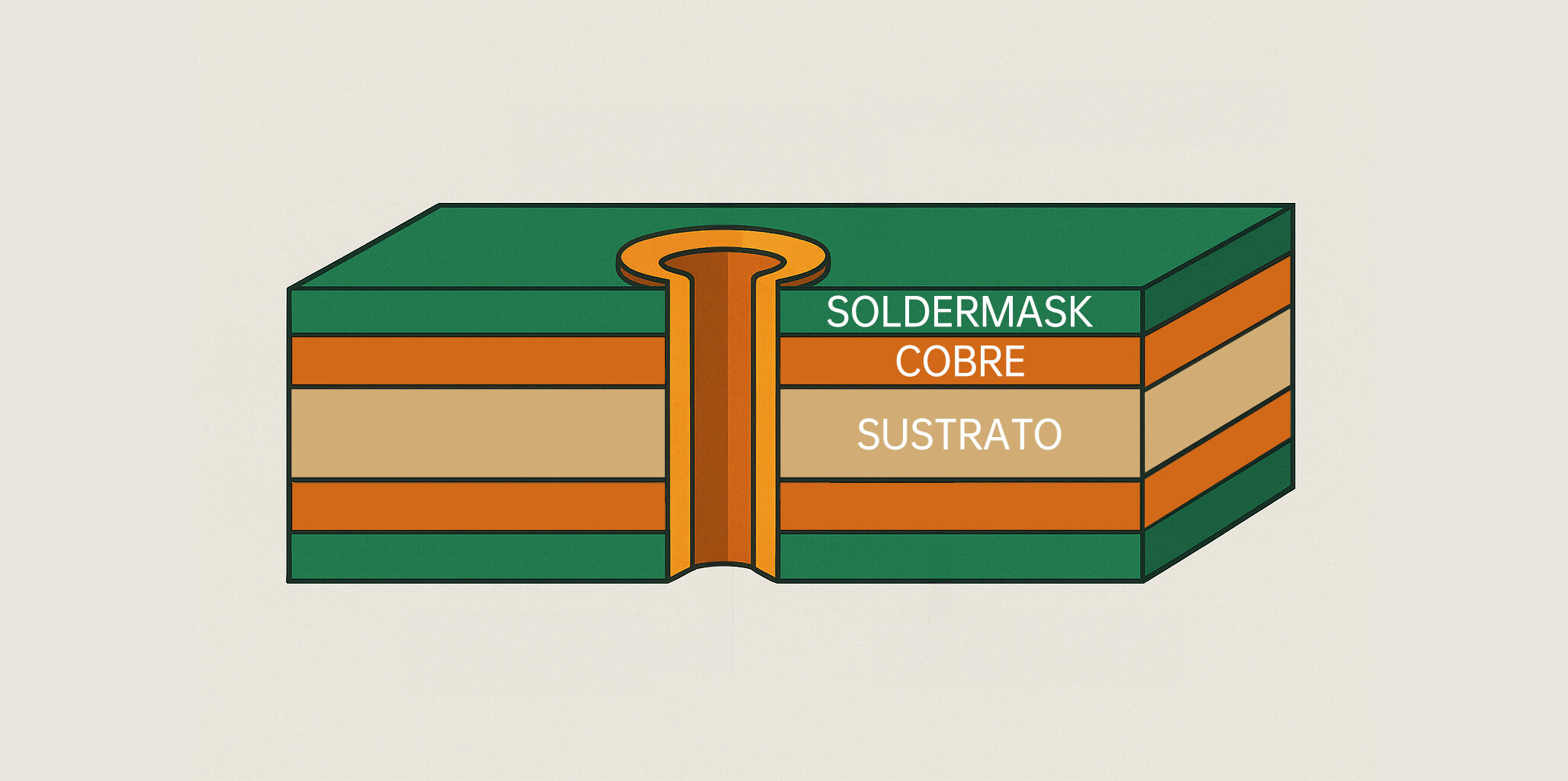
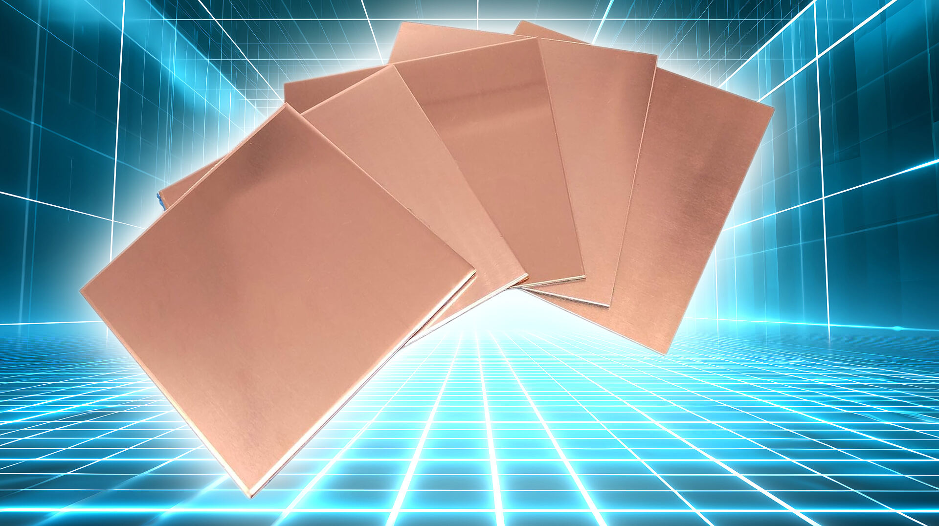
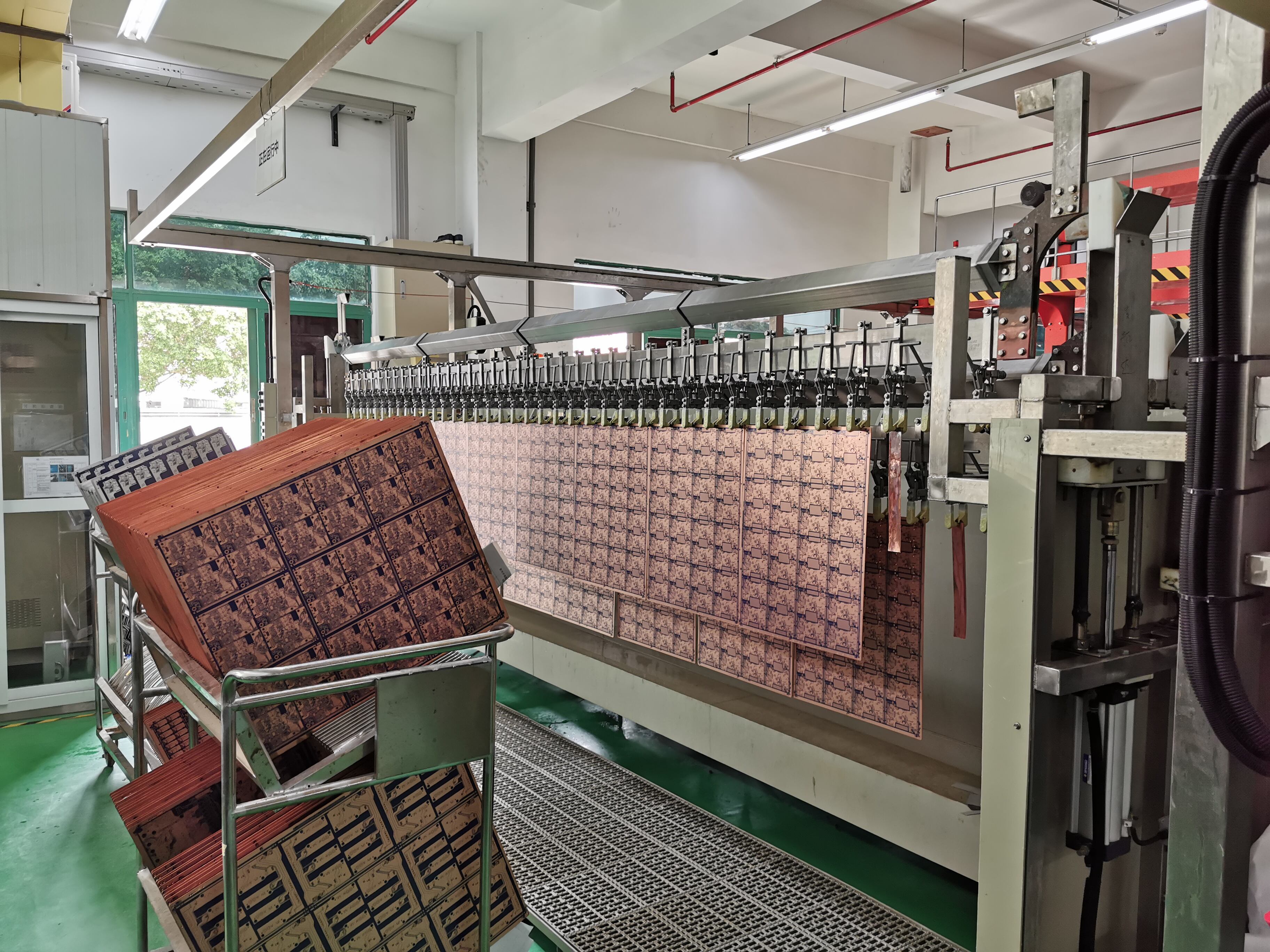
A gold finger PCB represents a sophisticated printed circuit board technology featuring gold-plated contact fingers along its edge, designed specifically for edge connector applications. These gold-plated contacts, typically measuring 30 microinches in thickness, ensure superior electrical conductivity and exceptional wear resistance. The gold plating process involves depositing a layer of nickel followed by a precise application of gold, creating a robust connection point that maintains its integrity through numerous insertion and removal cycles. These PCBs are extensively utilized in computer expansion cards, memory modules, and various plug-in devices where reliable electrical contact is paramount. The design incorporates beveled edges at specific angles, usually 30 degrees, to facilitate smooth insertion and prevent connector damage. The gold plating extends beyond the contact area to provide additional protection against wear and corrosion. Modern gold finger PCBs often feature impedance-controlled traces leading to the contact fingers, ensuring optimal signal integrity for high-speed applications. The manufacturing process includes rigorous testing protocols to verify both the plating thickness and the overall connection reliability, making these components essential in mission-critical electronics applications.