hdi circuit board
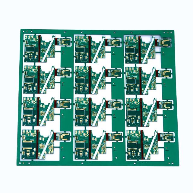
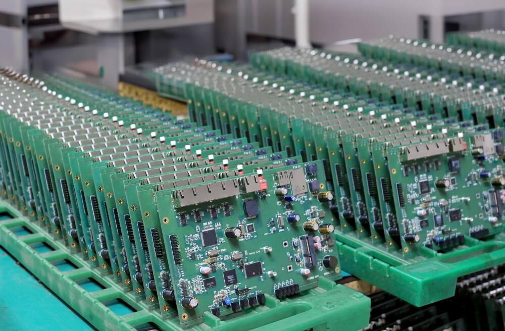
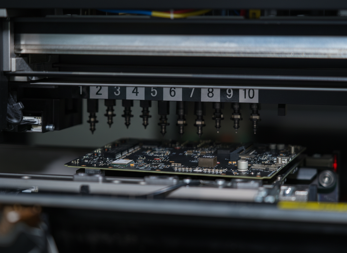
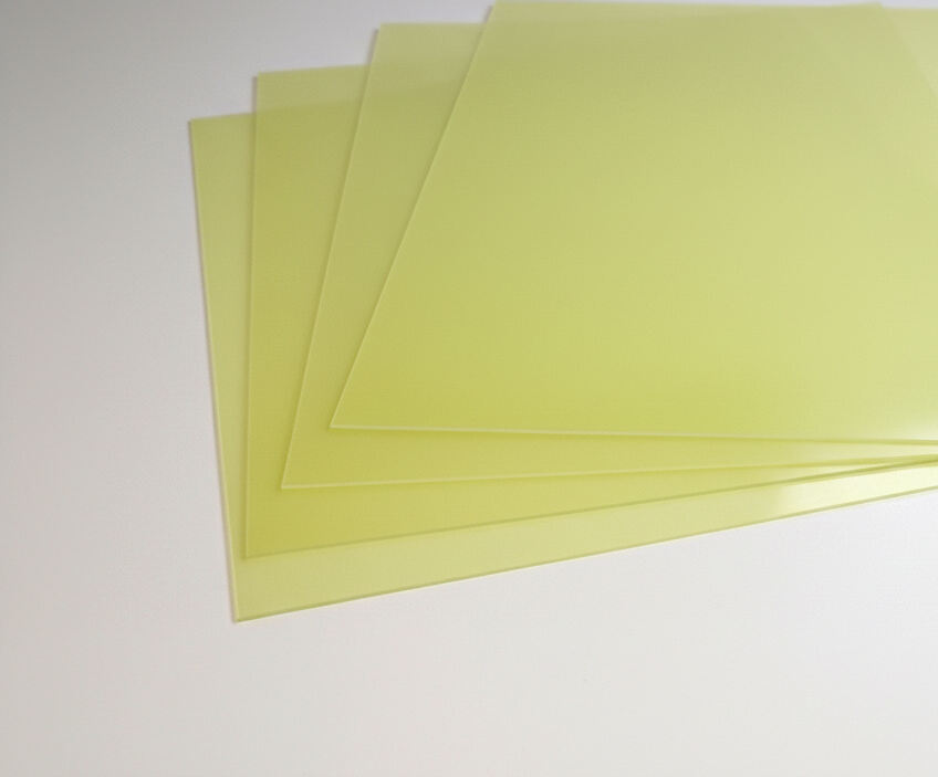
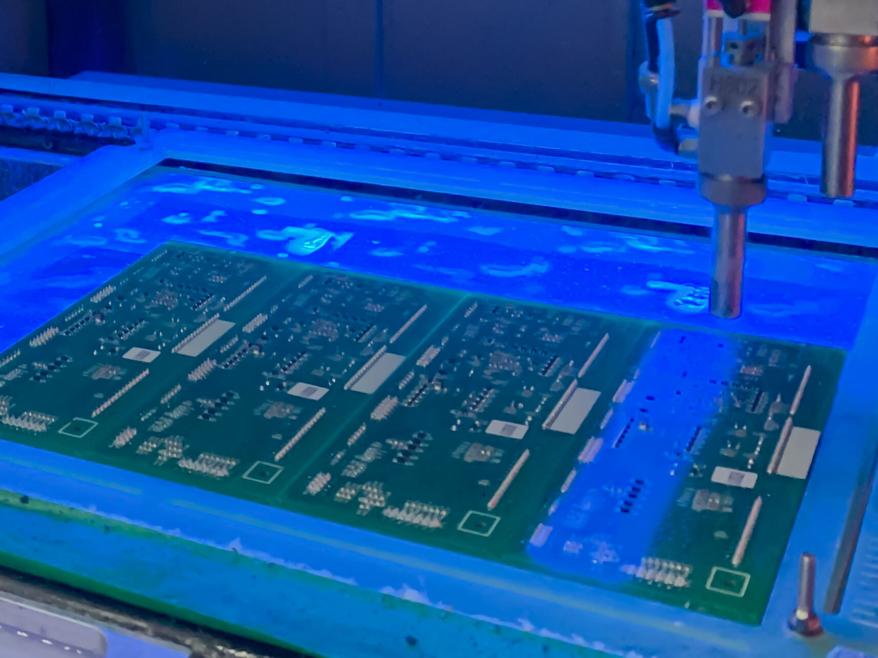
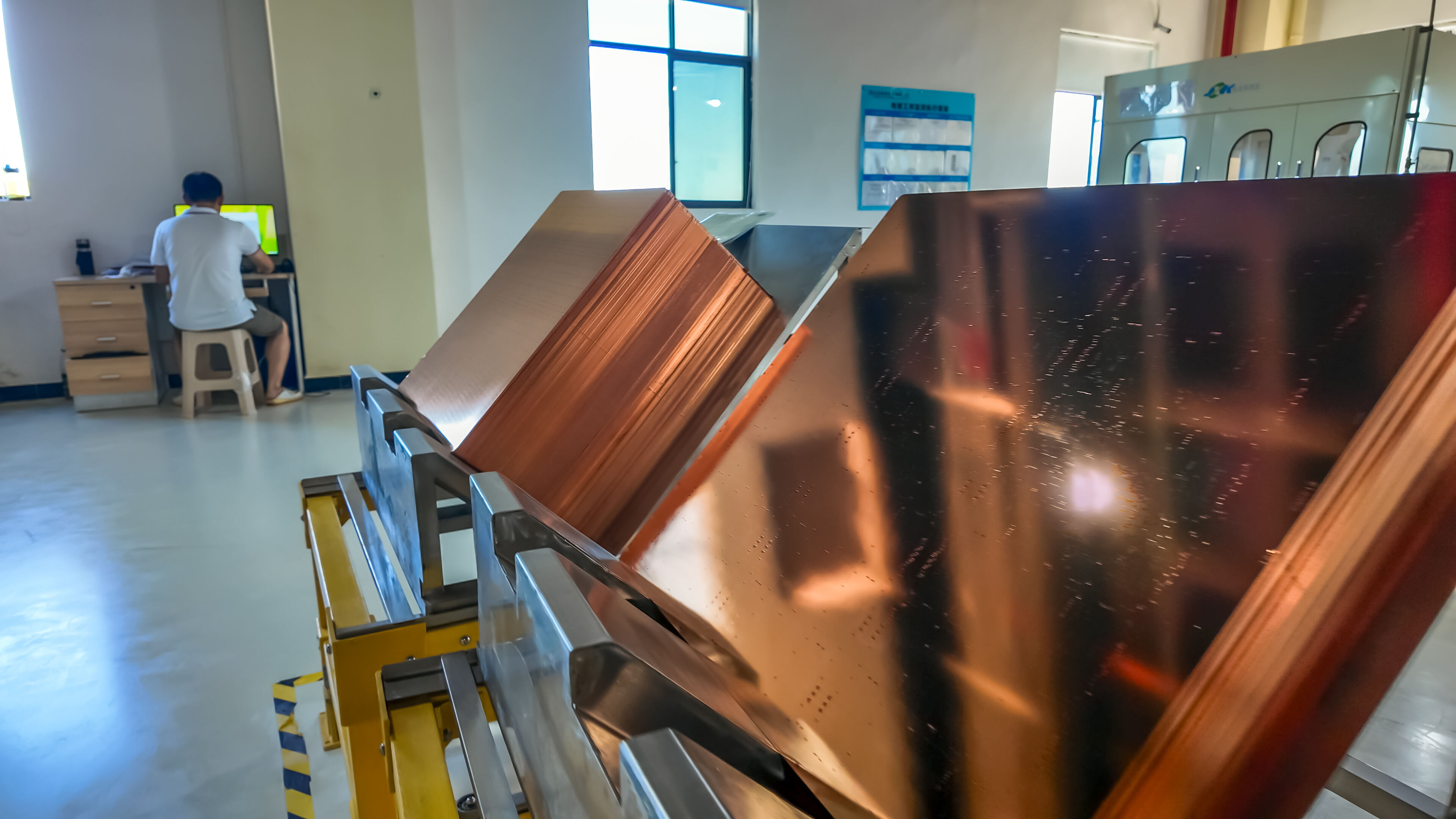
High Density Interconnect (HDI) circuit boards represent a cutting-edge advancement in printed circuit board technology, offering enhanced functionality in a compact form factor. These sophisticated boards feature increased circuitry density achieved through advanced manufacturing processes, including micro vias, blind vias, and buried vias. HDI circuit boards utilize finer lines and spaces, smaller vias, and higher connection pad densities than traditional PCBs, enabling more complex routing solutions in smaller areas. The technology incorporates multiple layers of thin dielectric material with laser-drilled micro vias, creating intricate interconnections between layers. HDI boards typically feature line widths and spacing under 100 microns, with via diameters less than 150 microns, allowing for significantly higher component density. This advanced design enables superior electrical performance, reduced signal loss, and improved signal integrity, making them ideal for high-frequency applications. The boards are widely implemented in smartphones, tablets, wearable devices, medical equipment, and other applications where space optimization and high performance are crucial requirements.