high density interconnect
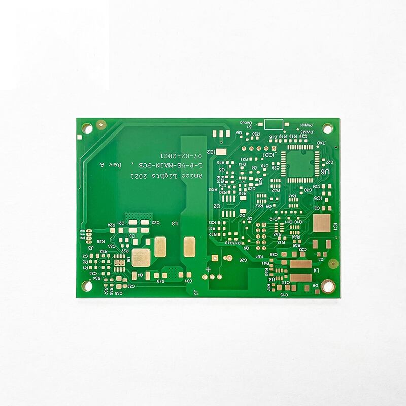
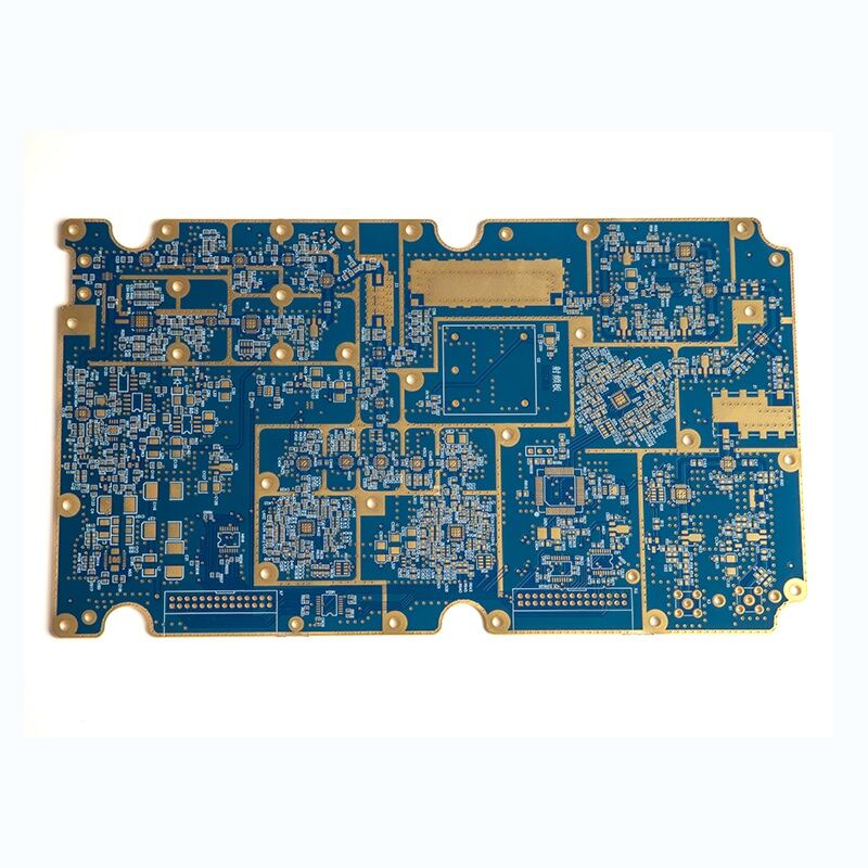
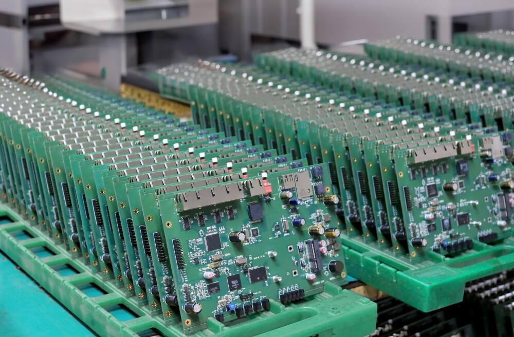
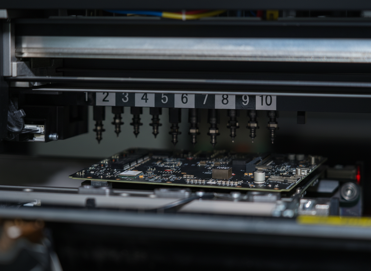
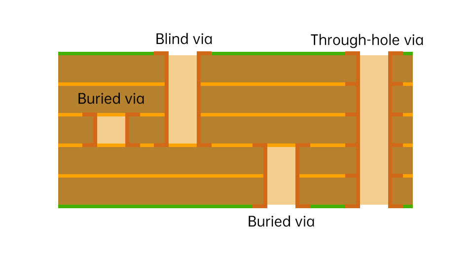
A high density interconnect (HDI) represents a cutting-edge printed circuit board technology that enables higher circuit density and more complex routing capabilities than traditional PCB designs. This sophisticated technology utilizes blind vias, buried vias, and microvias to create multiple interconnection layers, significantly reducing the overall size while increasing functionality. HDI technology achieves this by implementing finer lines and spaces, smaller vias, and higher connection pad density, allowing for more components to be placed in a smaller area. The technology typically features laser-drilled microvias with diameters less than 0.15mm, ultra-thin dielectric materials, and advanced manufacturing processes that ensure precise layer-to-layer registration. HDI boards are particularly valuable in modern electronic devices where space is at a premium, such as smartphones, tablets, and wearable technology. The architecture of HDI enables superior electrical performance by reducing signal path lengths, which minimizes signal delay and improves overall system performance. Additionally, these boards often incorporate advanced materials that offer better thermal management and signal integrity, making them ideal for high-frequency applications and devices requiring reliable performance in challenging environments.