high frequency pcb design
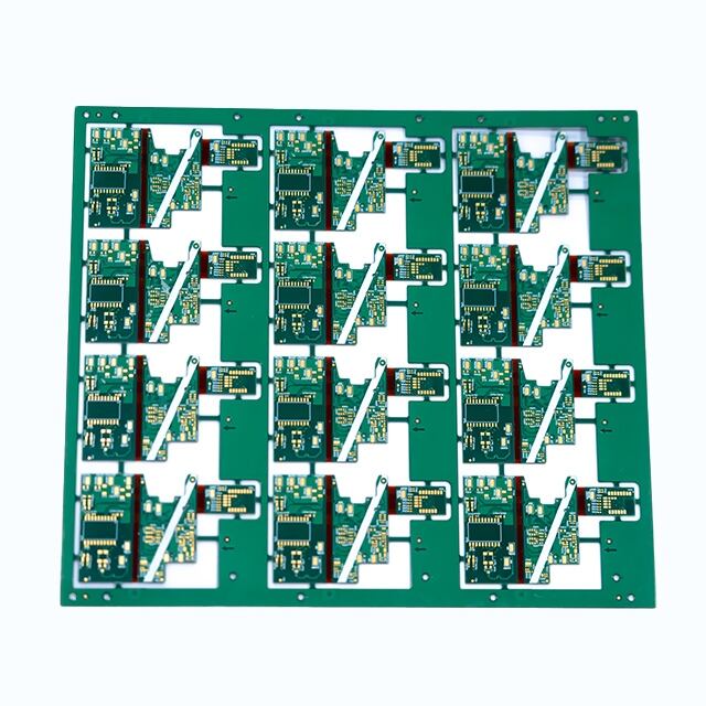
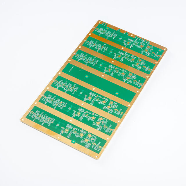
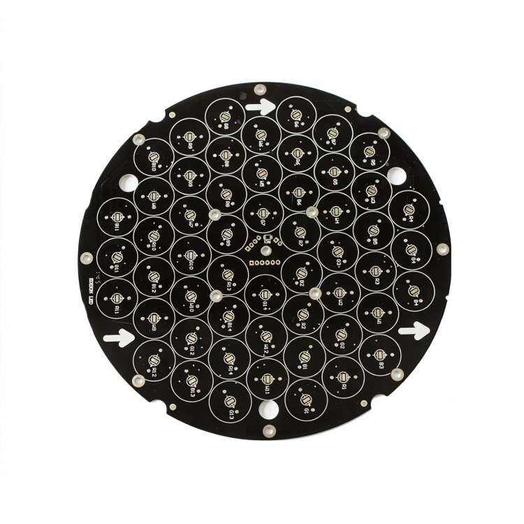
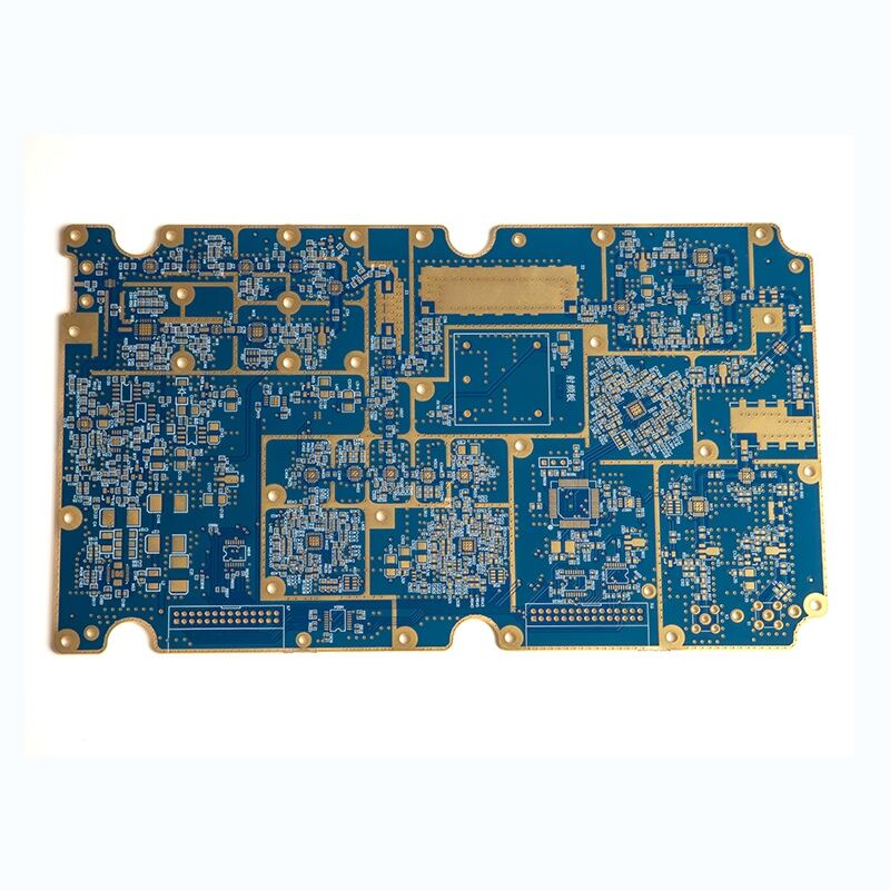
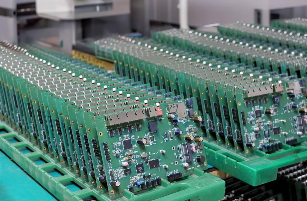
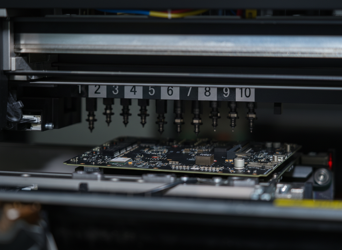
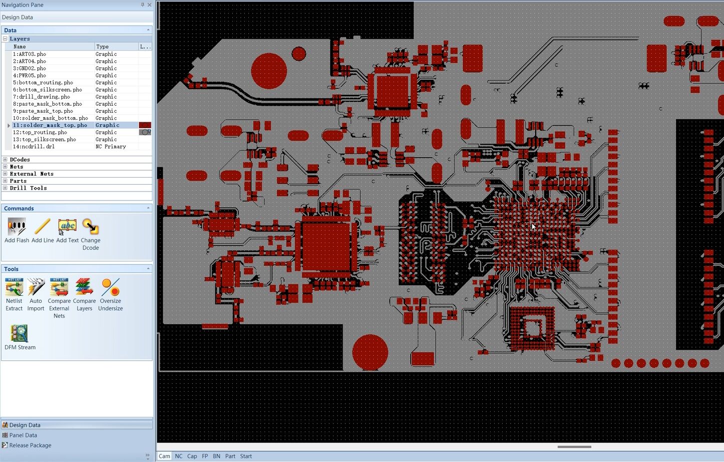
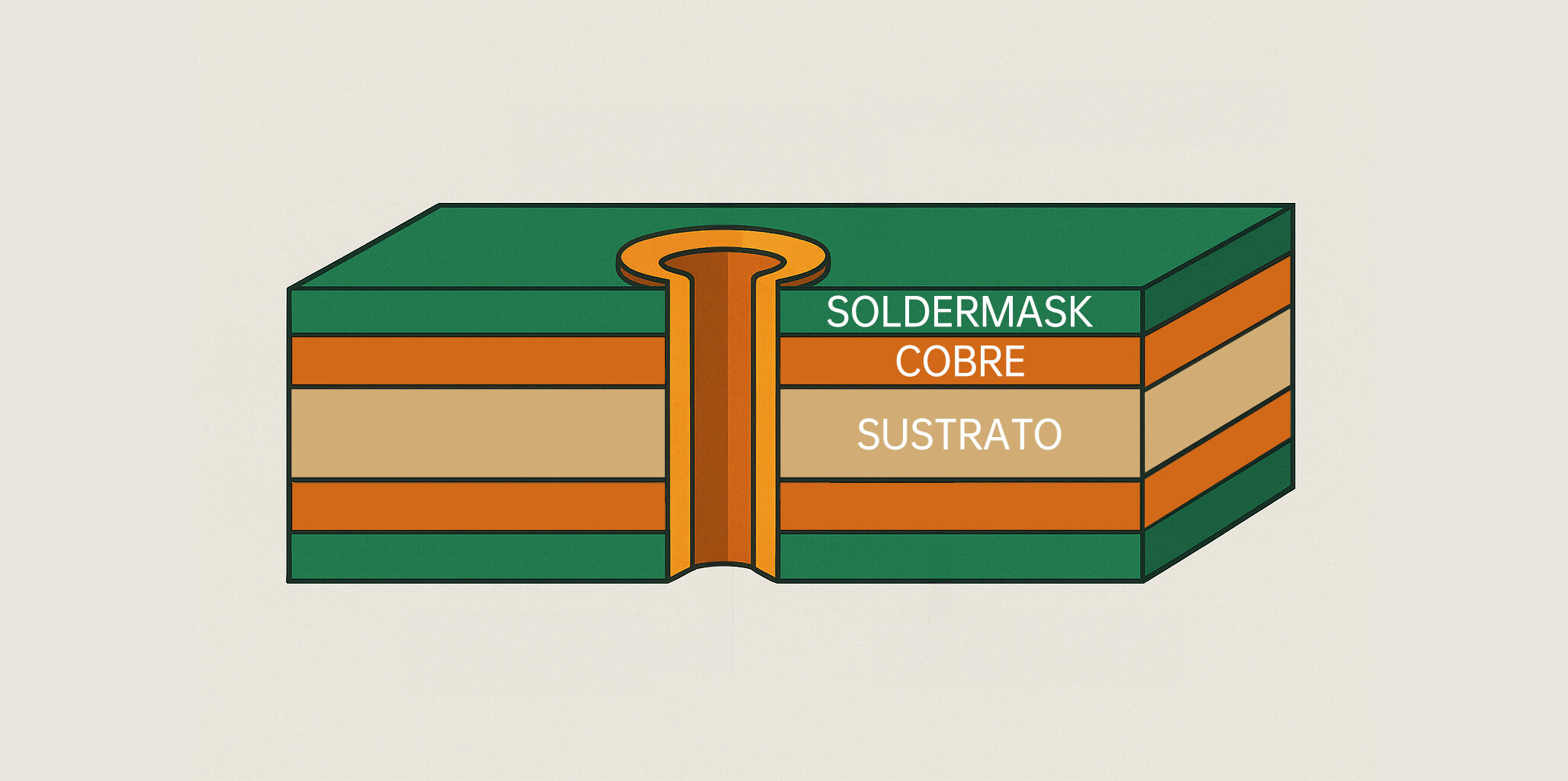
High frequency PCB design represents a specialized field in electronics manufacturing that focuses on creating circuit boards optimized for signals operating at frequencies typically above 100 MHz. These sophisticated designs require meticulous attention to detail, incorporating specific materials and layout techniques to maintain signal integrity and minimize electromagnetic interference. The main functions include efficient signal transmission, impedance control, and electromagnetic compatibility management. High frequency PCBs utilize specialized materials like Rogers, Taconic, or other low-loss substrates that offer superior electrical properties at elevated frequencies. The design process involves careful consideration of trace geometry, layer stackup, and component placement to minimize signal degradation and crosstalk. These PCBs find extensive applications in telecommunications equipment, radar systems, wireless devices, and high speed digital interfaces. The technology features advanced copper plating techniques, precise impedance matching, and controlled dielectric properties to ensure optimal performance. Modern high frequency PCB designs often incorporate advanced manufacturing techniques such as microvia technology, buried capacitance, and selective plating to achieve the desired electrical characteristics while maintaining manufacturing feasibility.