high density interconnect pcb
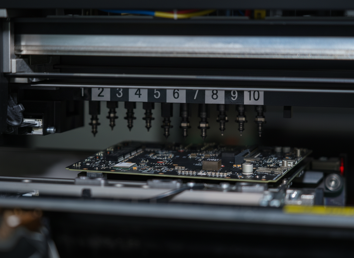
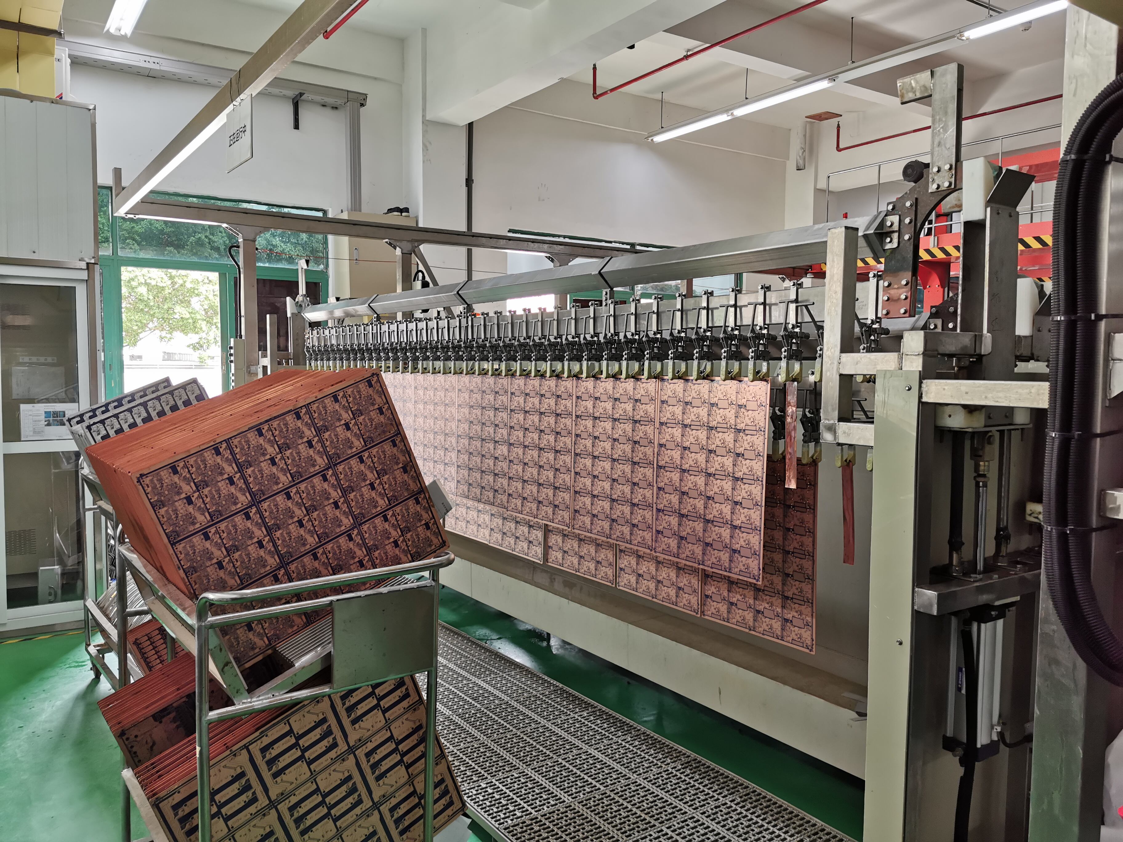
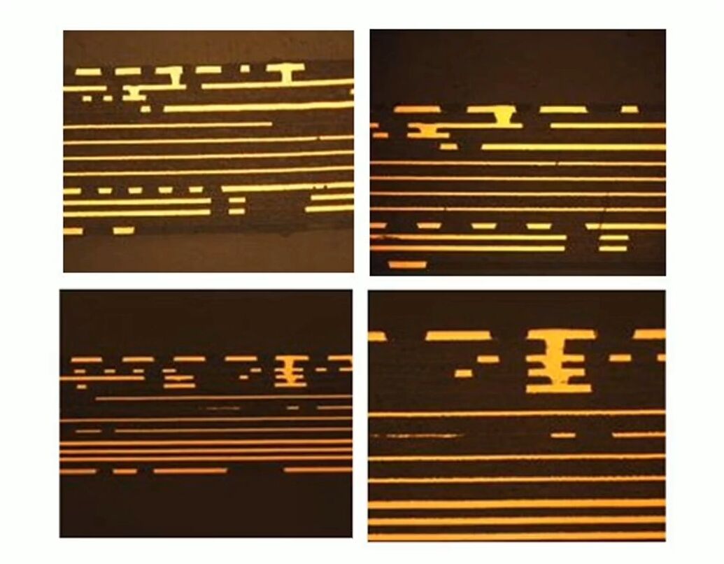
High Density Interconnect (HDI) PCBs represent a cutting-edge advancement in printed circuit board technology, offering superior electronic connectivity in a compact form factor. These sophisticated boards are characterized by their higher circuitry density per unit area, achieved through microvias, finer lines and spaces, and multiple layer interconnections. The core technology employs laser-drilled vias smaller than 0.006 inches in diameter, allowing for complex routing solutions in reduced spaces. HDI PCBs typically feature a higher number of connections per unit area, with line widths and spacing often less than 100 micrometers. These boards incorporate advanced manufacturing techniques, including sequential lamination processes and laser drilling, to create intricate interconnection patterns between layers. The technology enables the integration of more components in a smaller space while maintaining optimal electrical performance and signal integrity. HDI PCBs find extensive applications in smartphones, tablets, wearable devices, medical equipment, aerospace systems, and other high-performance electronic products where space is at a premium. Their ability to accommodate sophisticated IC packages and support high-speed signal transmission makes them indispensable in modern electronic design.