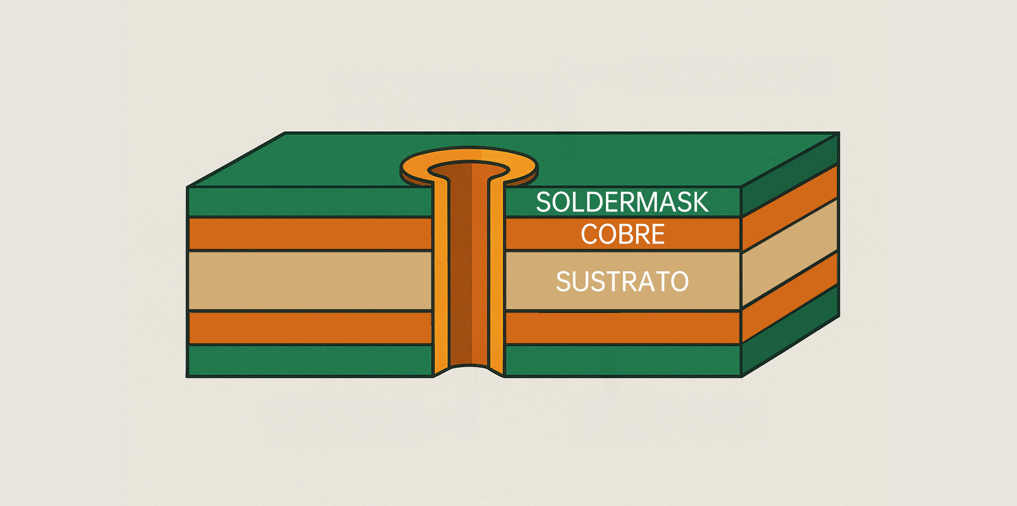
Blind Via Holes: Advanced PCB Technology for Enhanced Circuit Design and Performance

All Categories

blind via hole

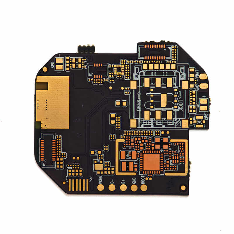
A blind via hole is a sophisticated PCB manufacturing feature that creates electrical connections between different layers of a printed circuit board without extending through all layers. Unlike traditional through-holes, blind vias start from an outer layer but terminate at an inner layer, enabling more efficient use of board space and enhanced design flexibility. These specialized holes are created using precise laser drilling or mechanical processes, allowing for the formation of reliable electrical pathways while maintaining the integrity of other board layers. The technology has become increasingly important in modern electronics, particularly in applications requiring high-density component placement and complex routing solutions. Blind via holes enable manufacturers to create more compact designs by reducing the space needed for interconnections, making them essential in mobile devices, wearable technology, and other miniaturized electronic products. The process involves careful consideration of aspects such as aspect ratio, plating requirements, and overall manufacturing feasibility to ensure optimal performance and reliability. This technology has revolutionized PCB design by offering enhanced signal integrity, improved thermal management, and better electromagnetic interference (EMI) shielding capabilities.

Popular Products

Blind via holes offer numerous compelling advantages in PCB manufacturing and electronic device design. First and foremost, they significantly enhance space utilization by eliminating the need for holes to traverse the entire board thickness, allowing for more efficient component placement and routing options. This space-saving characteristic is particularly valuable in modern electronics where miniaturization is crucial. The technology also provides superior signal integrity by reducing signal path lengths and minimizing potential interference between different layers. From a manufacturing perspective, blind vias offer greater flexibility in terms of layer stack-up design and component placement, enabling more complex and sophisticated circuit designs. The ability to create connections between specific layers without affecting others helps reduce electromagnetic interference and improves overall signal quality. Additionally, blind via holes contribute to better thermal management by allowing for more efficient heat dissipation pathways. They enable higher component density while maintaining reliable electrical connections, making them ideal for high-frequency applications. The technology also supports the implementation of advanced features such as impedance control and power distribution networks. From a cost perspective, while the initial manufacturing setup might be more complex, the long-term benefits in terms of reduced board size, improved performance, and enhanced reliability often justify the investment.

Tips And Tricks

Why Choose PCB Solutions for Industrial Applications?

09

Oct

Why Choose PCB Solutions for Industrial Applications?

The Evolution of PCB Solutions in Modern Industrial Landscapes The industrial sector has witnessed a remarkable transformation with the integration of advanced PCB solutions into its core operations. From automated manufacturing facilities to sophist...
View More
What Problems Can Happen in PCB Circuit Boards and How to Solve Them?

09

Oct

What Problems Can Happen in PCB Circuit Boards and How to Solve Them?

Understanding Common PCB Circuit Board Issues and Their Solutions PCB circuit boards are the backbone of modern electronics, serving as the foundation for countless devices we use daily. From smartphones to industrial machinery, these intricate compo...
View More
How Are PCBs Manufactured? Key Steps and Processes Explained

09

Oct

How Are PCBs Manufactured? Key Steps and Processes Explained

Understanding the Complex Journey of Circuit Board Production PCB manufacturing has revolutionized the electronics industry, enabling the creation of increasingly sophisticated devices that power our modern world. From smartphones to medical equipmen...
View More
Why Choose Professional PCB Manufacturing Services?

09

Oct

Why Choose Professional PCB Manufacturing Services?

The Critical Role of Expert PCB Production in Modern Electronics In today's rapidly evolving electronics industry, the quality and reliability of printed circuit boards (PCBs) have become more crucial than ever. Professional PCB manufacturing service...
View More

Get a Free Quote

Our representative will contact you soon.
Email
Name
Company Name
Message
0/1000

blind via hole

Enhanced Design Flexibility and Space Optimization

Enhanced Design Flexibility and Space Optimization

Blind via holes revolutionize PCB design by offering unprecedented flexibility in component placement and routing. This technology enables designers to create more compact and efficient layouts by utilizing connections that only span necessary layers rather than traversing the entire board thickness. The ability to target specific layers allows for optimized signal paths, reducing overall trace lengths and improving signal integrity. This feature is particularly valuable in high-density designs where every millimeter of board space counts. The technology enables the creation of more sophisticated multilayer boards while maintaining manageable manufacturing processes. By eliminating unnecessary through-holes, designers can achieve higher component density and more efficient use of available space, leading to smaller overall product dimensions without compromising functionality or reliability.
Superior Signal Performance and EMI Reduction

Superior Signal Performance and EMI Reduction

One of the most significant advantages of blind via holes is their contribution to enhanced signal integrity and reduced electromagnetic interference. By creating shorter, more direct paths between layers, these vias minimize signal degradation and reduce the potential for cross-talk between different circuit elements. The shorter signal paths result in decreased parasitic inductance and capacitance, leading to improved high-frequency performance. This characteristic is especially crucial in modern high-speed digital circuits where signal integrity is paramount. The technology also allows for better control of impedance matching and power distribution, resulting in more reliable and efficient circuit operation. The reduction in EMI helps ensure compliance with electromagnetic compatibility requirements while improving overall system performance.
Manufacturing Efficiency and Cost-Effectiveness

Manufacturing Efficiency and Cost-Effectiveness

While blind via holes require sophisticated manufacturing processes, they offer significant long-term benefits in terms of production efficiency and cost-effectiveness. The technology enables the creation of more compact designs, reducing material usage and overall product size. This reduction in size often translates to lower material costs and improved manufacturing yields. The ability to create targeted connections between specific layers also simplifies the overall board design process, potentially reducing development time and costs. Additionally, the improved reliability and performance characteristics of blind via holes often result in fewer field failures and warranty claims, contributing to lower lifecycle costs. The technology also supports automated manufacturing processes, helping to maintain consistent quality while reducing production time and labor costs.
Blind Via Holes: Advanced PCB Technology for Enhanced Circuit Design and Performance

Get a Free Quote

Our representative will contact you soon.
Email
Name
Company Name
Message
0/1000