Introduction
The printed circuit board (PCB) is at the heart of every electronic device, silently powering our phones, vehicles, medical equipment, and satellites. As China's production and manufacturing processes, capabilities and technologies for printed circuit boards continue to improve.However, even the highest-quality boards are not immune to one of the most persistent and costly failures in electronics: PCB delamination. When layers of the board begin to separate, electrical failures and product recalls often follow close behind.
Understanding PCB delamination and how to prevent it.First, it is necessary to understand that the causes of delamination can be roughly divided into four categories: material issues, manufacturing process problems, external environmental influences, and inappropriate chemical treatments, etc.If we look at it from a detailed perspective of the manufacturing process,but how humidity, thermal processing, assembly, and storage conditions interact. Defects such as delamination, measling, and crazing compromise the surface layer of a PCB and the inner structure, undermining reliability and sometimes safety.
What is PCB Delamination?

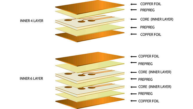
PCB (Printed Circuit Board) delamination refers to the phenomenon of delamination or separation between different layers of the circuit board during the production process.PCB delamination occurs when layers of the board—combinations of copper, resin, and substrate—begin to separate due to various mechanical, thermal, or chemical triggers. Delamination may manifest as bubbles or gaps, discoloration and bubbling, blisters, or even warping of the PCB surface layer.When stratification occurs, if left unchecked, delamination can lead to an uptake in humidity within the PCB, accelerating further damage,this leads to the loss of the pcb's functionality.
Judging from some commonly used materials,board materials like FR-4 material or polyimide are used as pcb base materials. These laminates, adhesives, and copper foils are highly engineered but remain vulnerable. When exposed to excessive humidity or subjected to thermal cycles, even top-grade laminate materials can lead to separation if not properly manufactured and handled.
PCB Structure |
Role |
Delamination Risk |
Copper Conductor Layer |
Carries signals |
May crack or blister if surface layer of PCB separates |
Dielectric Layer |
Insulation between layers |
Traps moisture, often first to “peel” away |
Laminate (FR-4/Polyimide) |
Bulk board material |
Incorrect type/Tg can cause delamination |
Surface Layer/Solder Mask |
Protection and isolation |
Delamination on the surface layer undermines pad/trace protection |
Why PCB Delamination is a Critical Issue
Why does delamination command so much attention in the world of PCBs? Simply put: If delamination happens, the entire PCB may fail.PCB serves as the fundamental component for signal and circuit transmission in the entire control board.
Why Delamination Is So Dangerous:
- Electrical Failures: The most direct one is conductor paths get interrupted; power or data is lost, and random faults result.
- Thermal Hotspots: Because the air gaps caused by delamination have low heat transfer, creating local “hot spots” that finally to accelerate further failure.
- Structural Weakness: From a structural perspective,when base PCB materials delaminated, lose mechanical strength and are prone to cracking, especially during assembly or rework.
- Long-Term Damage: Humidity in the PCB substrate keeps attacking from inside, leading to corrosion, measling, and further blistering.This is a factor caused by the external environment.
- Hidden Risks: Even if delamination may not stop a device initially, it shortens PCB lifespan—causing products to fail long before their intended end-of-life,and the PCB has lost its most fundamental performance.
Causes of PCB Delamination: The Main Factors
If you want to solve the problem of stratification, then start from the causes.
Understanding causes of PCB delamination and why delamination occurs is the first step to prevention.
1. Moisture Uptake & Humidity
PCB base materials are hygroscopic—The phenomenon of moisture absorption is usually closely related to factors such as the chemical structure and porosity of the materials used, as well as environmental humidity. Common PCB substrates, such as FR-4 (epoxy resin glass cloth composite material), have certain pores and can absorb moisture from the air.Meaning they absorb moisture from the environment, especially if the board is left unprotected in high humidity. Excess humidity in the PCB can be trapped in the PCB base and exposed to humidity during manufacturing, storage, or transportation. Later, exposure to high temperature during soldering cycles turns that moisture to steam.
- When moisture trapped in the PCB is heated past the boiling point of water, it creates powerful internal pressure. If the laminate can’t vent or absorb this pressure, the layers begin to separate and this leads to a decline in electrical performance, uneven thermal expansion, reduced mechanical strength, and even problems such as electrical short circuits and the last delamination occurs.
- Storage conditions of laminate materials are critical.When the humidity in the air increases, it also accelerates the adsorption of moisture. If the surface of the substrate absorbs moisture and the rate of moisture absorption increases with the rise in humidity. So failing to vacuum-seal or bake PCBs before assembly is a leading cause.
- Humidity in the PCB substrate can also cause measling (see below).
2. Thermal Stress & Thermal Processing

When the PCB enters the SMT assembly and processing stage every board undergoes repeated thermal stress during assembly. Thermal processing (reflow soldering, wave soldering, repair) heats the board above 200°C.After being affected by high temperatures if the laminate is old, has the wrong resin type, or isn’t baked, delamination may follow.
- Poor thermal profile or exceeding the resin’s specified Tg (Glass Transition Temperature, e.g., using FR-4 material with the incorrect type of Tg) are common triggers.Therefore, when selecting materials, the final application requirements of the product should also be evaluated, and an appropriate Tg grade should be chosen.
- Subjected to thermal cycling, the expansion and contraction of layers “works” the bonds loose, especially in HDI boards or those with thick copper conductors.
3. Manufacturing & Material Issues
- Poor manufacturing processes: Any particles, oils, or improper lamination during board pressing can always cause delamination.In today's fully automated production line workshops, this factor has been greatly reduced.
- Incorrect type of Tg: FR-4 or polyimide must match the actual thermal processing of your assembly.
- Old, out-of-spec board materials or expired resin can lead to delamination.It is recommended to use materials from commonly used international brands.
- Material with the incorrect type of Tg: If reflow consistently gets hotter than your substrate is rated for, delamination blister formation is only a matter of time.As mentioned above, choosing the appropriate substrate for Tg can reduce the probability of this problem.
4. Mechanical & Chemical Triggers
- Flexing the board, poor handling, or shocks will cause delamination, especially once bonds are weakened by moisture or heat.
- Cleaning agents, flux, and solder mask residues, if not cleaned correctly, can degrade the interface between the surface layer and base, setting the stage for delamination.
Mechanical & Chemical Triggers they are commonly seen in the later reprocessing and assembly production, caused by external factors.
Summary Table: PCB Delamination Causes
Cause Category |
Typical Trigger / Error |
Humidity/Uptake |
Trapped, unbaked, or exposed boards |
Temperature |
Too-hot profile, multiple reflow/wave soldering eyes cycles |
Manufacturing |
Poor press/lamination, expired resin, dirty surfaces |
Material Handling |
Incorrect Tg, out-of-spec supplies, poor storage |
Chemical |
Flux/cleaning agent residues, corrosive atmosphere |
Mechanical |
Excessive flex/shock during post-fab handling |
Measling and PCB Crazing: Related Forms of Delamination
Delamination, measling, and crazing are often confused but represent distinct defects in the world of printed circuit boards—each with its own set of risks and causes.These several quality issues not only affect the appearance of the PCB, but may also seriously impact its electrical performance and reliability.
Measling and PCB Defects
Measling is the formation of very small delaminated white spots, typically at the intersections of glass fibers in the PCB base material. These appear as fine white dots under the solder mask or laminate and are sometimes mistaken for early-stage delamination. Measling and PCB delamination have some relationship, as both result from breakdowns in laminate materials often triggered by excess humidity in the PCB or poor manufacturing processes.
- Measling are usually caused by oxidation or corrosion of the metal layer on the PCB surface (such as the copper layer), or moisture, or they may be due to inappropriate coating or surface treatment,especially when boards are exposed to rapid thermal changes or subjected to thermal shocks during soldering.
- When moisture is trapped in the PCB base materials or when materials undergo improper curing, small white spots emerge. Over time, these spots can grow, leading to more severe delamination if left unaddressed.
Crazing
Crazing is characterized by a web-like pattern of microcracks running through the base laminate of the PCB,it is commonly caused by material fatigue, improper control of the text and graphics during the welding process, and improper mechanical operations such as poor drilling and cutting.Unlike measling, which is localized, crazing often covers broader areas, creating a netted or mesh appearance beneath the solder mask. While crazing does not always cause delamination, it is a visible indicator of stress and can weaken the structural integrity of the board.
When Related Forms of Delamination Are a Concern
- Measling and crazing can lead to delamination if the board is further stressed by thermal or mechanical cycling, or if trapped moisture expands during assembly or product use.
- Boards displaying formation of very small delaminated white spots should be quarantined for further inspection and testing.Regularly conduct problem checks on materials or basic tests before use.
- By adopting scientific design, manufacturing and testing processes, the occurrence rate of these problems can be significantly reduced, and the reliability and long-term stability of PCBS can be enhanced.
Quick Comparison Table: Measling vs. Crazing vs. Delamination
Defect |
Visual Cue |
Main Cause |
PCB Impact |
Measling |
Small white spots at fiber bundles |
Humidity, cure issues |
Cosmetic if isolated, risky if widespread |
Crazing |
Fine, web-like cracks in laminate |
Thermal/mechanical cycling |
Often cosmetic, but weakens laminate |
Delamination |
Large blisters, bubbles, separation |
Heat, moisture, incorrect Tg, process |
Major—can cause full circuit or insulation loss |
Effects and Consequences of PCB Delamination
PCB, as a high-precision electronic material.If it consequences of delamination and its related forms in PCBs are far-reaching, affecting electrical, thermal, and mechanical aspects of a device.The most direct consequence is the decline in the mechanical and electrical properties of the sheet, and even functional failure.
Electrical Performance Issues
Short circuits and open circuits are the most common and also the routine diagnostic manifestations that best reflect the delamination phenomenon.
- Conductor Interruption: Where conductors or traces separate from the base material, circuits become open, leading to device malfunction or intermittent faults.
- Shorts and CAF: Delamination can lead to new pathways for conductive anodic filamentation (CAF), bridging soldering eyes or copper tracks.
Thermal and Structural Implications
Often during the welding process, delamination intensifies when exposed to heat. Or cracking and deformation are caused by external forces.
- Thermal Isolation: Blisters and gaps reduce heat flow, causing overheating and rapid localized degradation of components near delaminated zones.
- Mechanical Weakness: The board loses its ability to flex or withstand shock loads, leading to cracking and further large-scale delamination.
Moisture and Corrosion
The influence of substrates such as FR-4 and CM-1 absorbing moisture from the air in a high-humidity environment.
- Trapped moisture in the PCB not only causes expansion when heated but can also accelerate corrosion, particularly at exposed copper via holes or tracks at the delaminated region.
- Repeated exposure to high humidity and poor storage conditions of laminate materials enables continued degradation,than thus leading to.
Impact on Product Lifetime and Reliability
For a large-scale PCB manufacturer, although the optimization of the external environment and the management of operation norms have avoided the problem of delamination, once it occurs, it will have a huge impact on the lifespan of the PCB itself and the reliability of the end products.
- Delamination and its variants (measling, crazing) reduce the effective PCB lifespan and mean that even devices passing initial functional tests may begin to fail months or years later,it significantly shortened the product's service life.
- These hidden failures may cause costly recalls and damage to brand reputation, as devices fail unexpectedly in the field.
How to Tell If a PCB is Damaged (Symptoms and Types of Delamination)
The best way to solve problems is to prevent them.Knowing the symptoms of PCB delamination is crucial for early detection and mitigation,we can identify the problem through the following clues.
Visual Cues
- Discolored area under the solder mask often hints at moisture buildup or early delamination.
- Blisters or bubbles along the surface layer or at internal stacking points are direct indicators.
- Delamination blister: A swollen or spongy region that appears raised from the PCB surface.
- Small delaminated white spots: Indicative of measling, especially after thermal cycles.
Electrical and Functional Clues
- Sudden or intermittent failures, especially after the board endures high temperature cycles.
- Circuits fail after reflow or wave soldering eyes are bridged unexpectedly.
- Odd resistance readings or loss of continuity across copper traces.
Mechanical Cues
- Boards exhibit odd warping, flexion, or a sense of “sponginess” when handled near delaminated regions.
Why and How Delamination Occurs During Soldering and Thermal Processing
Each PCB has to go through a high-temperature assembly process,but delamination is particularly likely during high-temperature assembly steps, and several PCB delamination causes connect the dots between design, material, and process.Therefore, it can be summarized which links in the manufacturing and design of this pcb need to be optimized.
Soldering and Reflow as Triggers
- Thermal processing such as reflow and wave soldering exposes boards to temperatures above the boiling point of water (100°C) and sometimes over 250°C.This temperature is a challenging minimum value for the heat resistance of the pcb.
- Moisture trapped in the pcb base vaporizes, creating internal pressure,this situation occurs when there is residual moisture in the inner layer of the PCB.
- If the pressure exceeds the adhesive’s holding capacity, delamination will occur—especially at weakest areas like via entrances or the edge of copper pads.
Common Triggers for Delamination During Assembly:
- Inadequate or incorrect Tg in laminate materials (e.g., using FR-4 material with the incorrect type of Tg for lead-free soldering).In the requirements of pcb process manufacturing, it is particularly important to select the appropriate specification and model of base material.
- Boards not pre-baked or vacuum-sealed, exposed to humidity before soldering.In current manufacturing processes, this factor hardly constitutes an inducement. However, for the opened packaging materials, they should be consumed as soon as possible to avoid material loss.
- Poor-quality pcb base materials that have absorbed moisture or degraded.
Why Large-Scale Delamination May Result
- If delamination starts at one soldering point, it can propagate outward, leading to large-scale delamination that affects multiple layers of base material.
Types of Tests to Measure PCB Delamination
Rigorous types of tests to measure delamination are used throughout the PCB industry, allowing proactive detection and assurance of quality.
Key Test Methods
Test Type |
Purpose/Result |
Scanning Acoustic Microscopy (SAM) |
Reveals voids, blisters, and gaps invisible to the naked eye |
Thermomechanical Analysis (TMA) |
Determines expansion characteristics, ID’s weak spots under temperature change |
Solder Float Test |
Assesses stability under high-heat, boiling solder conditions |
Interconnect Stress Test (IST) |
Measures via and plating integrity under repeated heat cycles |
Microsection Analysis |
Directly inspects cross-sectioned layers for internal voids |
Methods to Prevent Delamination and Solutions
Protection from delamination is multi-pronged, relying on design, storage, processing, and even supplier relationships.
Design & Material Choice
- After understanding the final performance and application of the material,than select FR-4 material or alternative PCB materials with appropriate Tg and moisture resistance.
- If the product is used in high humidity environments, PCBA assembly in progress use enhanced resins or apply protective conformal coatings.
Manufacturing and Processing Controls
- Maintain strict humidity control in storage and fabrication areas,strictly control the operation rules and regulations.
- Bake all boards to remove moisture before soldering, especially before high-temperature or multiple-pass assemblies.
- Audit suppliers for raw material traceability and require material with the correct type of Tg.
Assembly Best Practices
- Use correct profiles so that the surface layer of a PCB and copper never exceed manufacturer’s ratings.
- Allow cooling between thermal cycles to minimize expansion/contraction fatigue.
Safe Handling
- Educate staff on gentle handling wear gloves to avoid microcracks.
- Inspect regularly for measling, blisters, and minor delaminated areas,once any abnormal materials are detected, they should be immediately classified into the unusable materials area and ordered to be stored.
Environmental Control
- Use climate-controlled warehouses for storage conditions of laminate materials.
- Monitor with humidity and temperature sensors to avoid uptake in humidity.
PCB Delamination Repair Steps
If delamination has occurred, the function of some materials can still be restored through professional repair:
- Diagnose using visual inspection or SAM.
- Stop further handling (to prevent propagation of bubbles or gaps).
- Clean the area carefully—avoid aggressive cleaning agents that dissolve adhesives.
- Drill a tiny relief hole if needed to inject epoxy into the delaminated region.
- Inject high-spec epoxy and apply compressive pressure.
- Cure under controlled temperature to restore adhesion.
- Retest using electrical continuity and stress tests.
Frequently Asked Questions
Q: What is the main reason for delamination in modern multilayer PCBs?
A: The main factors that can lead to delamination today are uncontrolled humidity in PCB substrate and storage, using laminate materials with an incorrect or insufficient Tg for the assembly process, and poor manufacturing or lamination practices.
Q: How can I prevent delamination if PCBs must undergo multiple soldering or rework cycles?
A: Use a high-Tg board material, monitor humidity closely, vacuum-seal between processes, and bake boards before re-exposing them to high temperatures.
Q: Does every discolored area or bubble indicate critical delamination?
A: Not every visual anomaly requires scrapping. Small delaminated white spots (measling) may not always cause delamination, but always monitor for spreading. Discoloration often signals trapped moisture—address root causes before assembly continues.
Q: What is the difference between measling, crazing, and delamination?
A: Measling is the formation of small white spots, crazing presents as a network of fine cracks, and delamination is when actual physical separation or blisters occur in the PCB’s laminate or between copper and substrate.
Q: Can improper cleaning agents cause delamination?
A: Yes—especially aggressive solvents may degrade adhesion at the surface layer of the PCB or between layers, eventually causing delamination.
Q: Why do certain board areas delaminate more than others?
A: Delamination often begins at thermal or mechanical stress points—edges, via clusters, or around soldering eyes—especially where conductor density is high or where layers have lower adhesive strength.
Q: What types of tests should be part of our incoming and outgoing QC for PCBs?
A: Use microsection analysis, TMA, IST, SAM, and solder float testing to measure both potential and existing delamination in all critical lots. Always document and trend failure types.
Conclusion and Best Practices Recap
PCB is an electronic material processed with high precision. It has very high requirements and standards for material selection and storage, process control, and vacuum packaging and storage of finished products. Delamination is a complex failure mechanism resulting from moisture, material selection, poor manufacturing processes, and improper thermal processing. Tragedies such as large-scale delamination, sudden field failures, and recall events all stem from these main causes of PCB delamination,after identifying the problem, choose an appropriate solution,and minimize losses to the greatest extent possible.
Your Delamination Prevention Checklist:
- Always use the right board materials that have the proper, certified Tg rating for your specific process temperatures.
- Keep a tight control on how and where you store laminate materials, and make sure all PCBs—coming in or going out—are handled following strict climate rules.
- Set up humidity monitoring, and don't skip the pre-bake step, especially for boards that might have soaked up moisture.
- Pick suppliers who have solid certifications for their processes and materials, and check in on them regularly.
- Train every person handling or assembling boards on what delamination is and how to stop it—that means teaching them to spot and report anything that looks or acts unusual.
- Run strong, reliable tests to check for delamination as part of your normal process checks and final quality control.

