Introduction

The surface finishing process of PCBs can not only maximize the solderability and comprehensive performance of Printed Circuit Boards (PCBs), but also form a protective barrier to prevent the copper surfaces of PCBs from oxidative corrosion. It can further effectively extend the overall service life of PCBs and ultimately ensure that the delivered PCB products fully comply with the relevant standards formulated by the industry.There are numerous surface finishing processes in the current industry, among which Hot Air Solder Leveling (HASL) and Electroless Nickel Immersion Gold (ENIG) are the two core technologies with the widest application scope and highest frequency of use.Both of these two processes have their own advantages and disadvantages.This guide will systematically explore the core differences, technical characteristics and application features between the two processes of Hot Air Solder Leveling (HASL) and Electroless Nickel Immersion Gold (ENIG). It will ultimately provide you with clear reference basis to help you accurately select the most suitable PCB surface finishing process based on your specific requirements in the PCB design and manufacturing links.
The Importance of Surface Finishes in PCB Design and Manufacturing
Surface treatment plays a critical role in the design and manufacturing processes of printed circuit boards (PCBs). This process effectively protects the exposed copper pads on PCBs from oxidation by preventing direct contact with air. The selection of an inappropriate surface treatment method will directly compromise solder joint reliability and adversely affect electrical conductivity. A uniform protective coating must be applied to the PCB surface to ensure the formation of high-quality solder joints and extend the board's overall lifespan.
Surface Mount Technology (SMT) stands as one of the core processes in electronics manufacturing. Surface treatment processes serve as the critical foundation ensuring stable SMT operation. These processes create smooth and flat soldering surfaces for SMT applications, guaranteeing stable and precise placement of microelectronic components. Therefore, selecting the appropriate surface treatment method directly determines the final outcome of the PCB manufacturing process, exerting a decisive influence on board quality, assembly efficiency, and ultimate product reliability.
There are many types of PCB surface treatment processes, each possessing unique advantages along with specifically suitable application scenarios. Therefore, when selecting the optimal process, multiple factors must be comprehensively taken into account, including cost constraints, shelf life, operational environment, component spacing, and relevant regulatory requirements.
The most commonly used surface treatment methods include:
1. HASL (Hot Air Solder Leveling)

- Leaded HASL: Traditional processes using tin-lead alloys are being phased out because they do not meet safety and RoHS standard.
- Lead-free HASL: This process uses tin-copper alloy or tin-silver-copper alloy, which are standard components for most new circuit boards.
2. ENIG (Electroless Nickel Immersion Gold)

- This surface treatment process first deposits a layer of electroless nickel plating, followed by a thin layer of immersion gold. The ENIG process creates a smooth, flat surface, making it ideal for surface mount technology (SMT) and small-pitch components.
3. OSP (Organic Solderability Preservative)
- OSP is a surface treatment process that protects copper by coating its surface with an organic compound before the first soldering. This process is cost-effective but has limited durability.
4. Immersion Tin
- Immersion tin, also known as white tin plating, can create a fine, smooth, and uniform surface. It is ideal for surface mount technology (SMT), but its lifespan is limited by the risk of tin whiskers.
5. Immersion Silver
- This surface treatment is similar to immersion tin, offering excellent solderability and good electrical properties, but its surface is prone to oxidation and discoloration.
6. Hard Gold (Electrolytic Gold)
- This process is mainly used for edge connectors such as "gold fingers" and has excellent wear resistance.
7. ENEPIG (Electroless Nickel Electroless Palladium Immersion Gold)
- This multi-layer surface treatment not only provides ENIG with excellent corrosion resistance, but also makes it suitable for wire bonding and soldering.
In-Depth Look at HASL Surface Finish
Hot Air Leveling (HASL) remains one of the most widely used surface treatment processes in PCB manufacturing. It is regarded as an ideal solution for numerous standard applications due to its dual advantages of cost-effectiveness and reliable performance. The particular popularity of HASL in medium-to-low complexity PCB designs warrants further examination, which I will delve into next.
What is HASL?

Hot Air Leveling (HASL) is a surface treatment process employed in printed circuit board (PCB) manufacturing, whose core operation involves depositing a layer of molten solder onto the copper pads of the PCB. This process establishes a structurally stable and reliable soldering foundation on the pad surfaces, thereby ensuring smooth execution of subsequent soldering operations. Furthermore, it creates an effective protective layer on the board's copper surfaces that blocks direct contact with atmospheric oxygen, thus effectively preventing oxidation-related degradation of the circuit board.
Process
- Prepares the PCB by cleaning copper surfaces.
- The board is dipped into molten solder.
- Hot air leveling can make the solder surface smooth and ensure that the exposed copper layer is evenly covered by solder.
- The board is cooled and sent for final inspection.
Types of HASL
- Leaded HASL: Although this process remains common in some regions and in traditional applications, it does not comply with RoHS standards.
- Lead-free HASL: It is the preferred surface treatment process for modern environmentally friendly electronic products and has a very wide range of applications.
Advantages and Disadvantages of HASL
Advantages:
- HASL offers significant cost advantages compared to other surface treatments, making it ideal for prototyping and mass production.
- HASL provides excellent solderability for through-hole components and large SMT components.
- Hot air leveling (HASL) is ideal for circuit boards that do not require high flatness or spacing.
- This surface treatment method is easy to inspect and supports both manual and automated methods for identifying assembly defects.
Disadvantages:
- HASL may not be able to provide the smooth, uniform surface required for BGA and fine-pitch surface mount devices.
- Whether Leaded and lead-free HASL are used, will result in uneven coating thickness and surface roughness.
- For high-frequency or high-performance applications, signal integrity and surface flatness are critical, and HASL is not the optimal PCB surface treatment process.
- In high-temperature or humid environments, the durability of HASL coatings is inferior compared to other surface coatings.
- Leaded HASL does not meet environmental protection requirements and is therefore being phased out by lead-free alternative processes.
When to Use HASL
- HASL is ideal for cost-sensitive designs that use large-pitch and through-hole components and do not require very fine pitch compatibility.
- If the design is a prototype or will be assembled shortly after production, use HASL to prevent oxidation.
HASL and ENIG: Differences and Similarities
While both processes are generally familiar to professionals, PCB designers should recognize that the fundamental differences between HASL and ENIG manifest across multiple dimensions:
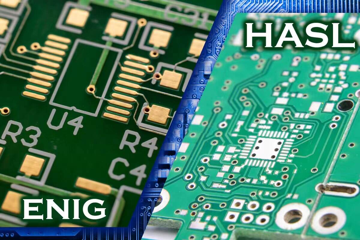
- HASL surface treatment is cheaper than ENIG, but the surface smoothness is not as good as ENIG.
- ENIG's excellent smoothness and corrosion resistance make it an important material for applications requiring smooth surfaces and long shelf life.
- The choice between HASL and ENIG surface treatments depends on the circuit board layout, assembly process, and regulatory requirements.
Spotlight on ENIG Surface Finish
What is ENIG?

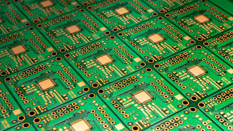
ENIG is a surface treatment process that deposits a layer of nickel onto copper and then immerses it in gold. ENIG surface treatment is favored for its smooth, flat surface and compatibility with fine-pitch packages, BGA, and HDI designs.
The ENIG Process
- The PCB undergoes cleaning and micro-etching to expose a new copper layer.
- Electroless nickel plating is used to form a uniform nickel layer.
- A thin layer of gold is deposited on nickel using an immersion plating process, which effectively prevents oxidation.
Why ENIG Offers Superior Performance
- ENIG's flat surface makes it ideal for surface mount technology and soldering requirements of fine-pitch components.
- ENIG surface treatment offers excellent corrosion resistance, ensuring a longer shelf life for PCBs and maintaining stable performance even in harsh environments.
- ENIG surface treatment not only ensures excellent flatness of the welded surface, but also exhibits superior durability and supports multiple welding and rework cycles.
- ENIG surface is RoHS compliant by default.
- Although ENIG surface treatment may cost more than hot air leveling (HASL), the investment is worthwhile in terms of yield, reliability and performance for many advanced component requirements.
Advantages and Disadvantages of ENIG
Advantages:
- ENIG offers a flat, smooth solder surface, making it ideal for BGA, fine-pitch SMD, and HDI layouts.
- Minimize the tombstone effect and open seams in surface mount manufacturing.
- ENIG is very durable and more resistant to corrosion and oxidation than HASL or OSP.
- It has a long shelf life and excellent compatibility with modern welding processes.
- There is no risk of lead contamination, and it always complies with RoHS standards.
Disadvantages:
- ENIG is more expensive than other surface treatment processes, especially compared to HASL.
- If not handled by a reputable PCB manufacturer, a "black pad" defect may occur.
- Due to the fragility of the gold layer and the complexity of the process, its reworkability may not be as good as HASL.
When to Use ENIG
- PCB designers should specify ENIG surface treatment when working with fine-pitch components, BGA packages, HDI boards, or sensitive analog/RF applications, as these design scenarios demand superior surface performance and precision.
- ENIG is the best choice when you need a long PCB lifespan, stable soldering performance, and environmental compliance.
- Selecting the appropriate PCB surface treatment is critical to the board's performance and application effectiveness. While ENIG may involve higher costs compared to HASL, its exceptional long-term reliability makes it the preferred process in aerospace, medical equipment, telecommunications, and high-end consumer electronics industries.
Benefits of ENIG
- This process ensures an extremely smooth surface and enables highly precise positioning.
- This process ensures the reliability of SMT assembly and minimizes the risk of soldering defects.
- ENIG surface treatment processes provide smooth, uniform surfaces, which are crucial for ensuring signal integrity in high-speed circuits and minimizing signal loss and reflection.
- ENIG surface treatment is also suitable for wire bonding processes and edge connector applications that require gold plating.
- ENIG surface treatment is highly compatible with automated optical inspection (AOI) because its surface smoothness and reflectivity make it easier to identify weld defects.
HASL vs ENIG: Detailed Comparison

The selection between HASL and ENIG surface treatment processes requires comprehensive consideration of multiple factors, including PCB performance requirements, project budget constraints, actual assembly processes, and the end-product's application fields. A detailed comparative analysis of these two processes will now be presented:
Criteria |
HASL Surface Finish |
ENIG Surface Finish |
Cost |
Lower; HASL is cost-effective |
ENIG is more expensive compared to other surface finishes |
Flatness |
Uneven; not suitable for very fine pitch |
ENIG offers a flat surface, ideal for BGA & fine-pitch |
Solderability |
Good for PTH, large SMDs; easy to rework |
ENIG finish allows superior solderability, less reworkable |
Environmental Compliance |
Lead-free HASL is RoHS compliant, leaded is not |
ENIG is always RoHS compliant |
Shelf Life |
Moderate |
ENIG offers a long shelf life |
Resistance to Corrosion |
Moderate |
Excellent; gold protects the nickel and copper |
Technical Complexity |
Simple, widely used |
Complex, requires expert fabrication controls |
Suitable Applications |
Prototyping, basic/consumer electronics, automotive |
Medical, telecom, aerospace, high-end consumer, RF/HDI |
Risk of Manufacturing Defects |
Thicker finish, risk of bridges and uneven joints |
Black pad possible; flat, reliable finish with correct QC |
Key Differences Between HASL and ENIG:
- HASL technology is typically used when cost is the primary criterion and flatness is less important.
- ENIG is a surface treatment process that produces a smooth, flat surface suitable for high-density designs.
- The HASL process offers better rework convenience, while ENIG provides better soldering performance for small or sensitive parts.
- Although ENIG is more expensive than HASL, it is undoubtedly the best choice for many applications, especially those that require long lifespan and reliability.
- ENIG is known for its compliance and superior performance, making it a popular choice in modern PCB design and manufacturing for advanced, long-life, or globally distributed products.
Other Surface Finish Options for PCB Projects
While most designers typically choose between HASL and ENIG, there are actually many other options for PCB surface treatment processes:
- OSP: This process is cost-effective for certain SMT assemblies, especially suitable for small-batch scenarios requiring rapid assembly.
- Immersion Tin: This process can meet the requirements of a smooth surface and lead-free process, but has a shorter shelf life.
- Immersion Silver: This process is well-suited for high-speed, high-frequency applications, but its storage and management conditions require strict control.
- Hard Gold (Electrolytic): This process is often used for edge connectors due to its abrasion resistance, but its primary purpose is not to provide solderability.
- ENEPIG: This process adds a palladium layer to the ENIG base, further enhancing its advantages and eliminating the risk of black pads, making it an ideal choice for military or medical hardware.
In certain special circumstances, these alternative processes may be the best option, and designers should consult with reliable PCB manufacturers to fully evaluate all feasible options.
Factors to Consider When Choosing the Right PCB Surface Finish

The following key parameters need to be considered when selecting a suitable circuit board surface treatment process:
- PCB Design Features: The optimal PCB surface treatment solution depends on three key technical factors: pad spacing, in-pad via process, and the use of BGA-type microsphere components.
- Assembly Process: Surface mount technology, reflow soldering process and potential rework requirements.
- Regulatory Compliance: Does your product need to comply with RoHS, REACH, or IPC Level 2/3 standards?
- Production Volume and Timeline: Cost per board, and how long boards will be stored before assembly.
- Operating Environment: Moisture, temperature, vibration, and possible field repairs.
- Expected Lifetime: The lifespan of printed circuit boards, especially for critical industrial, automotive, or aerospace systems.
- Cost Constraints: Find the product with the best cost performance without sacrificing necessary quality or compliance.
- Supplier Expertise: Your options may be limited by manufacturing capabilities and the level of process control (especially for ENIG).

Tips for Selecting the Right Surface Finish for Your Project
- Consult Early with Fabricators: Some PCB manufacturers have proven their capabilities with ENIG, while others may recommend HASL, OSP, or ENEPIG depending on your design priorities.
- Evaluate Prototype Results: Small-batch trials were conducted using HASL and ENIG surface treatment processes to verify weld quality, appearance defects, and long-term oxidation.
- Prioritize Compliance and Longevity: For global, medical, automotive, or aerospace projects, ENIG and ENEPIG surface treatment processes are often the best choice, as their overall performance is significantly better than HASL and OSP.
- Balance Cost and Flatness: For simple, low-density prototypes, HASL is an ideal, cost-effective option; however, for high-value, fine-pitch, or long-life products, the additional investment in ENIG becomes a necessary choice to ensure product reliability.
- Consider Storage and Logistics: If the PCB needs to be stored for a long time before assembly, avoid using OSP and HASL; instead, choose the ENIG process, which provides long-term protection against oxidation and ensures solderability.
- Request Certifications: In critical applications, it is essential to obtain compliance certificates, shelf-life test data, and process control records—especially ENIG (which is a core quality control step in preventing black pad issues).
- Use Visual and Automated Inspection Data: In large-scale manufacturing, the compatibility of ENIG with automated optical inspection should be fully utilized to achieve mass production.
Industry Trends in Surface Finishes for PCBs
- Miniaturization and Fine Pitch Domination: As designers continue to pursue higher levels of integration, ENIG and ENEPIG have become the inevitable choice for cutting-edge circuit boards due to their superior performance.
- Environmental Regulations and Sustainability: Lead-containing HASL is being phased out at an accelerated pace globally. ENIG and other lead-free surface treatment processes have now become mainstream in all markets.
- Improvements in Automated Inspection: With the widespread application of AOI (Automated Optical Inspection) and X-ray solder joint inspection, higher requirements have been placed on the flatness and reflectivity of PCB surfaces, which is another reason for the increasing popularity of ENIG surface treatment technology.
- Focus on Reliability Over Cost Alone: As electronic devices permeate all areas, from transportation to implants, people's focus is shifting from simple cost to lifespan, maintainability, and user safety.
Frequently Asked Questions about HASL and ENIG
Q: What are the main advantages and disadvantages of choosing between HASL and ENIG?
A: The HASL process is affordable and flexible, but it has limitations in terms of fine-pitch components and lifespan. The ENIG process, on the other hand, provides a flat, reliable, and environmentally friendly surface, but it is more expensive and requires experienced manufacturers.
Q: When should I use HASL or ENIG?
A: The HASL process is suitable for prototyping, small-batch production, and orders with higher budgets. The ENIG process is suitable for high-density products, products with long shelf lives, or products that comply with relevant regulations.
Q: Can a surface finish affect the electrical performance of my PCB?
A: Yes, surface treatment affects solderability, signal loss, impedance matching, oxidation, and the overall quality of the printed circuit board. Compared to HASL, ENIG is particularly suitable for high-speed, high-precision circuits.
Q: Is ENIG always the best PCB surface finish for every project?
A: While ENIG surface treatment offers excellent flatness, corrosion resistance, and long lifespan, it's not necessary for all PCB projects due to its higher cost. For designs using only large-pitch components or simple through-hole technology, HASL surface treatment is a good choice due to its lower cost and ease of rework. However, for BGA, HDI, or boards operating in harsh environments, ENIG surface treatment is the optimal solution for ensuring best assembly yield and long-term reliability.
Q: What are the most common defects associated with each finish?
A: For the HASL process, common defects include solder bridges (due to uneven surface treatment) and inconsistent pad heights, which complicate the assembly of small-pitch components. For the ENIG process, the most significant defect is the "black spot" phenomenon, a type of nickel corrosion that can hinder solder joint formation if process control is not rigorous.
Q: How do I choose the best PCB surface finish for my product's lifecycle?
A: The optimal surface treatment for a printed circuit board (PCB) depends on its entire lifecycle: Does the PCB require international shipping? Does it need long-term storage? Will it be exposed to high humidity or frequent temperature fluctuations? In these cases, the choice between HASL and ENIG is crucial. ENIG provides reliable protection for international shipping and long-term storage, while HASL is suitable for on-demand assembly and less demanding applications.
Conclusion: Choosing the Best PCB Surface Finish
Choosing the right PCB surface treatment process requires weighing various factors, such as technical, economic, and logistical requirements. While HASL and ENIG are two of the most commonly used surface treatment processes for modern PCBs, their actual performance can vary significantly depending on project requirements.
- HASL (Hot Air Solder Leveling) is a widely used surface treatment process suitable for projects with low cost requirements, simple processes, or low requirements for surface flatness. This process is compatible with most SMT and through-hole components, making it a very good choice for users looking to reduce production costs.
- ENIG (Electroless Nickel Immersion Gold) is a surface treatment process that provides a smooth surface, excellent corrosion resistance, environmental compliance, and superior solderability for demanding printed circuit board (PCB) design and manufacturing projects. While ENIG is more expensive than high-adhesion silver (HASL), its greater durability, higher production yield, and longer shelf life make it an ideal surface treatment for high-reliability, high-density, and high-value PCBs.
Key Takeaway Table:
Parameter |
HASL Surface Finish |
ENIG Surface Finish |
Cost |
Low |
High |
Surface Flatness |
Uneven |
Smooth and Even |
Solderability |
Good for most parts |
Excellent, even for fine-pitch |
SMT & BGA Compatibility |
Moderate |
Superior |
Environmental Compliance |
RoHS with lead-free |
Always RoHS |
Shelf Life |
Up to 6 months |
12+ months |
Visual Inspection |
Easy |
Very easy (AOI) |
Reworkability |
Highly reworkable |
Moderate |
Corrosion Resistance |
Moderate |
High |
Defect Risks |
Bridges, thickness |
Black pad (rare with process control) |
Final Tips for Choosing the Right PCB Surface Finish:
- Consult your printed circuit board manufacturer as soon as possible; they will guide you in choosing the surface treatment method that suits your project's technology and market.
- For products requiring fine-pitch SMD, HDI, or long shelf life, the reliability offered by ENIG is simply unmatched by HASL.
- For prototyping, amateur electronics production, or printed circuit boards with large pad spacing and simple requirements, HASL remains one of the most cost-effective options.
- When selecting a PCB surface treatment process for your application, be sure to choose the solution that best meets product performance requirements, environmental adaptability, and compliance standards.
In the rapidly evolving electronics industry, selecting the right PCB surface treatment process is a core skill that every engineer and purchasing professional must master. Whether prioritizing performance, compliance, cost, or long-term durability, understanding the advantages and disadvantages of HASL and ENIG surface treatments can help you make accurate decisions and ultimately produce PCB products that exceed expectations.
