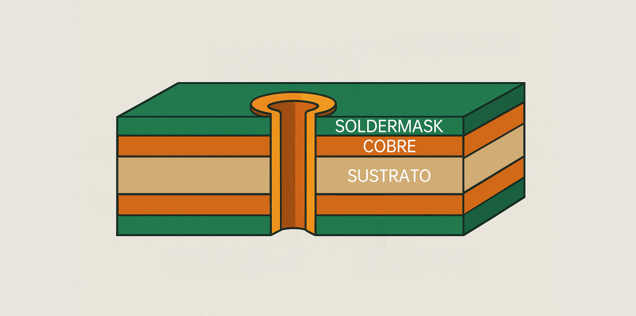
in pad via
An in pad via is a sophisticated technological component used in printed circuit board (PCB) manufacturing that creates electrical connections between different layers of a circuit board. This innovative design feature consists of a conductive pathway that passes through a pad, allowing for vertical electrical connections while maintaining signal integrity. The structure typically includes a copper-plated hole that connects multiple layers of the PCB, surrounded by a conductive pad on each layer. This configuration enables efficient use of board space and supports complex routing solutions in multilayer PCBs. The in pad via technology has become increasingly important in modern electronics, particularly in applications requiring high-density component placement and sophisticated signal routing. It supports both through-hole and blind via configurations, offering flexibility in design and manufacturing. The technology is particularly valuable in ball grid array (BGA) applications, where space is at a premium and direct connections between components and power or ground planes are essential. Modern in pad via designs often incorporate filling and plating techniques to ensure reliable connections and prevent manufacturing issues such as solder wicking.