Pad in Via Technology: Advanced PCB Solutions for Enhanced Performance and Reliability

All Categories

pad in via

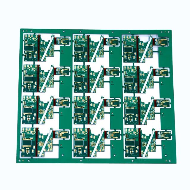
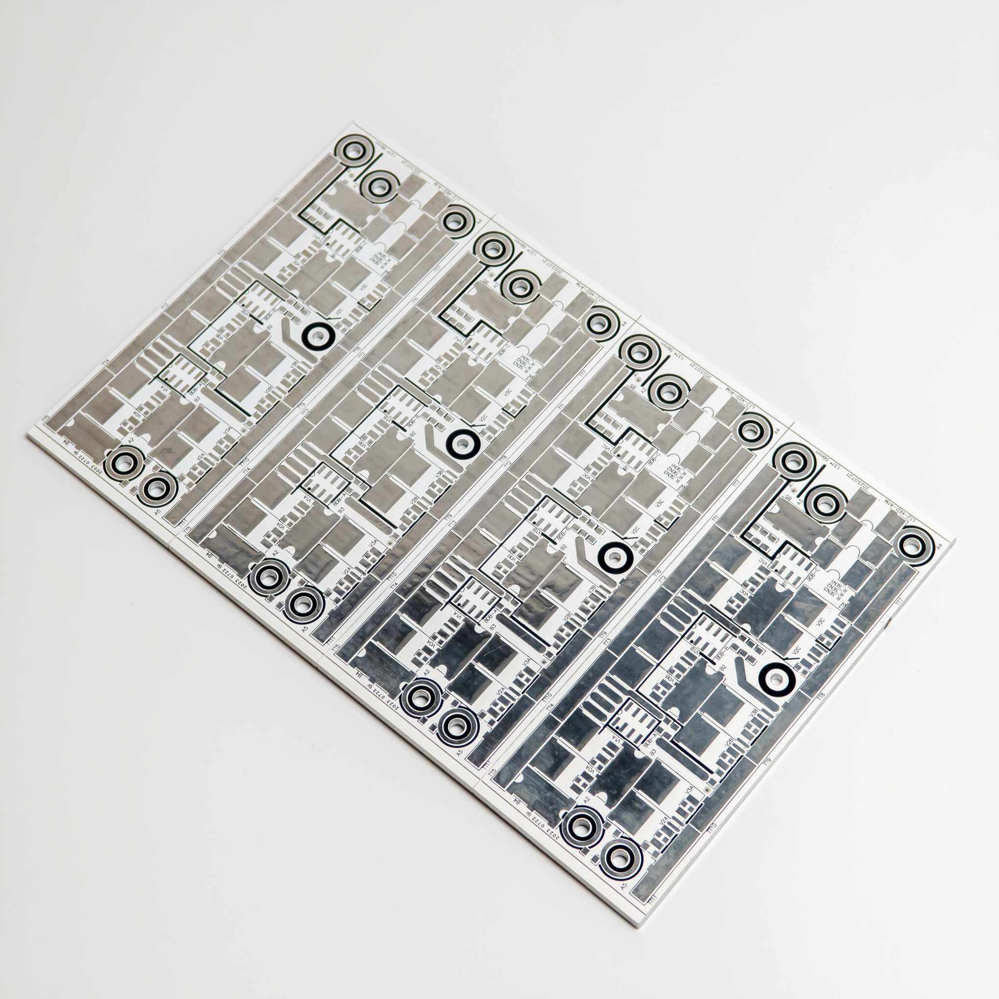
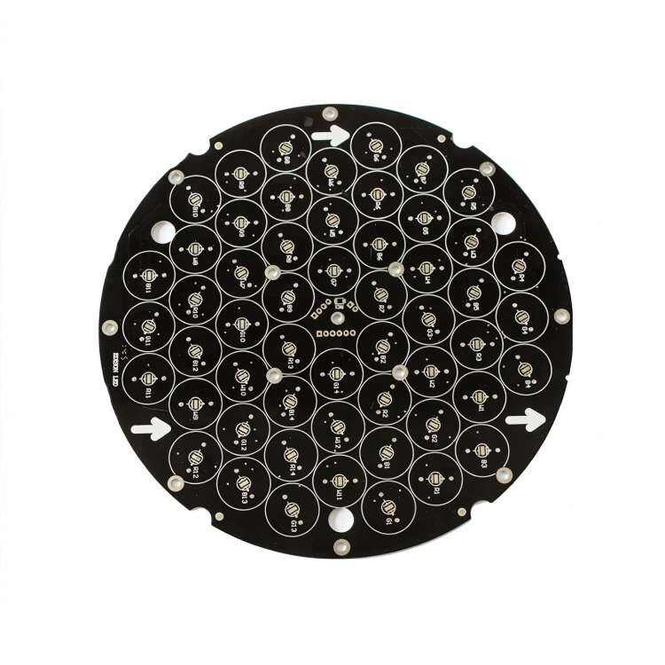
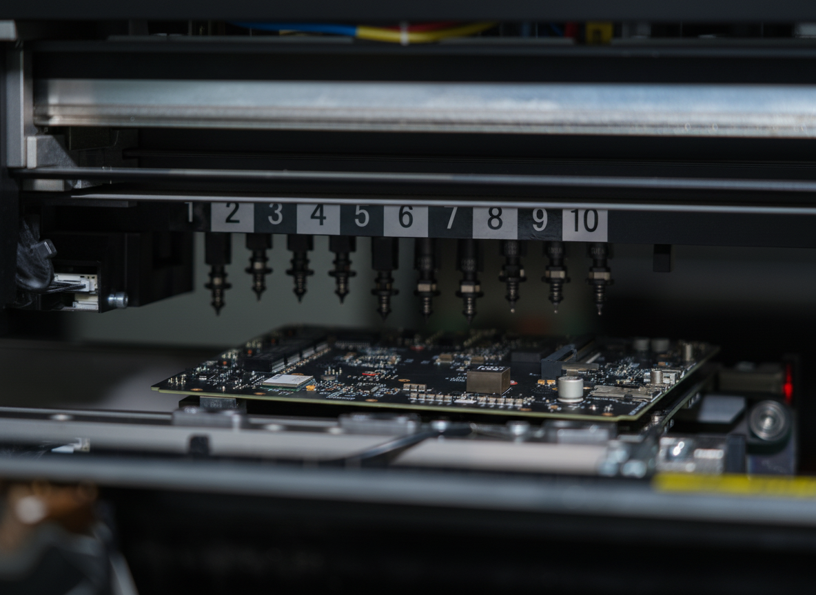
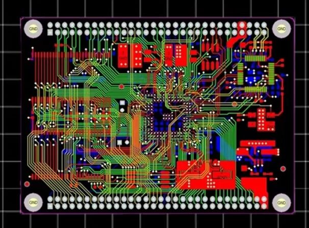
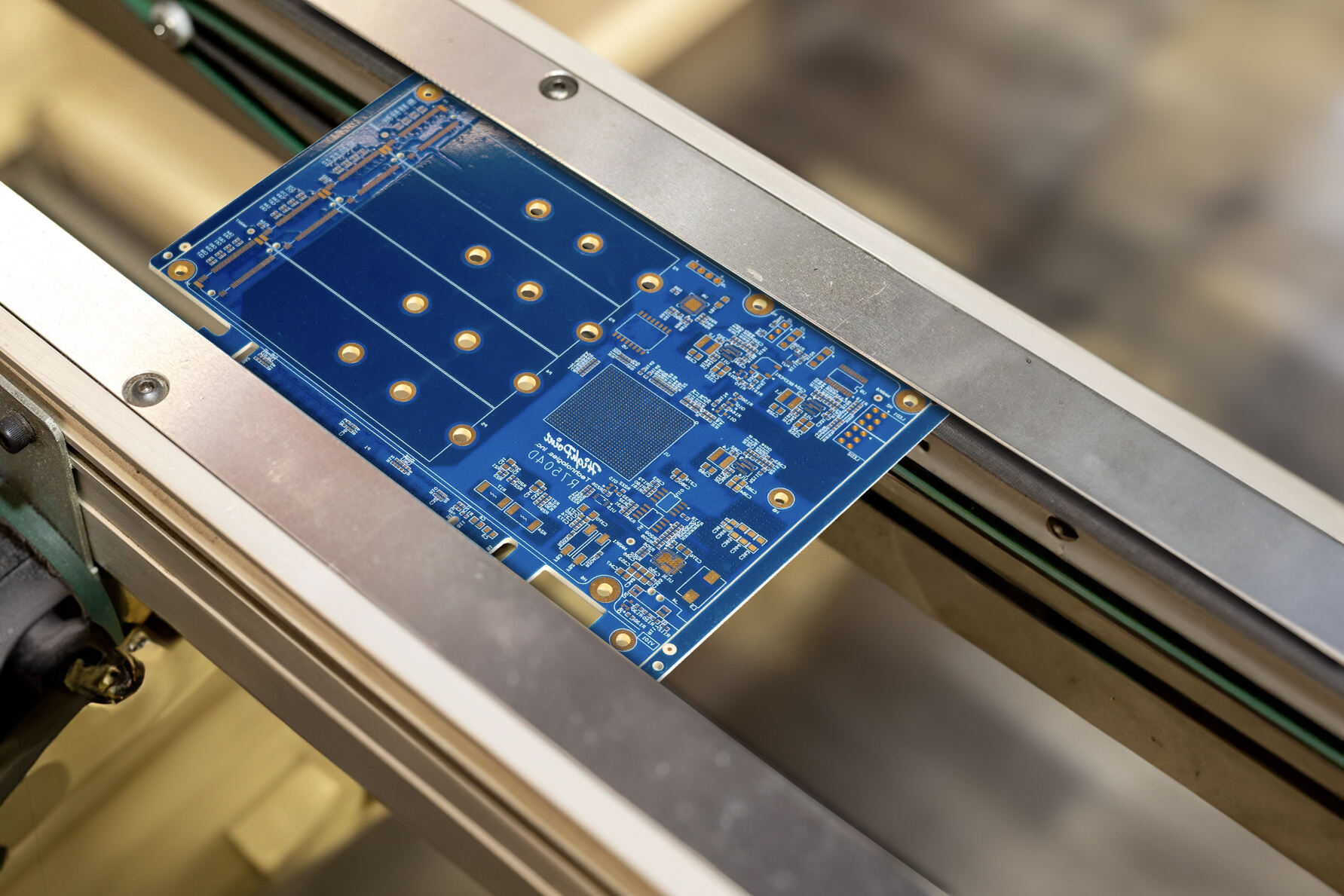
A pad in via is a crucial component in printed circuit board (PCB) design and manufacturing that serves as an electrical connection point between different layers of a circuit board. This specialized structure consists of a conductive pad surrounding a plated through-hole, creating a reliable electrical pathway while providing mechanical stability. The pad in via technology enables complex multilayer PCB designs by facilitating vertical interconnections between various circuit layers. The structure typically includes a copper pad on the surface layers connected to a metallized hole that extends through the board. Modern pad in via designs incorporate advanced features such as thermal relief patterns to manage heat distribution and optimize soldering processes. These components are essential for creating high-density electronic devices, as they allow for efficient use of board space while maintaining signal integrity. The technology has evolved to support various applications, from simple two-layer boards to sophisticated high-frequency designs, offering flexibility in PCB layout and improved manufacturing yields.

New Product Recommendations

The implementation of pad in via technology offers numerous significant advantages in PCB manufacturing and performance. First, it provides superior electrical connectivity between different board layers, ensuring consistent signal transmission and reduced signal loss. The design allows for more efficient use of board space, enabling higher component density and more compact overall designs. From a manufacturing perspective, pad in via structures offer enhanced mechanical strength, particularly important for components subject to mechanical stress or thermal cycling. The technology supports better thermal management by facilitating heat dissipation through the metallized holes, crucial for high-power applications. Additionally, pad in via designs contribute to improved signal integrity by reducing electromagnetic interference and minimizing cross-talk between adjacent traces. The technology enables greater design flexibility, allowing engineers to optimize circuit layouts for specific applications while maintaining manufacturability. These structures also enhance the reliability of solder joints, particularly in surface-mount technology applications, by providing additional mechanical anchoring. Furthermore, pad in via technology supports advanced PCB features such as buried and blind vias, enabling even greater circuit density and complexity when required.

Tips And Tricks

What Are the Different Types of PCBs and Their Applications?

09

Oct

What Are the Different Types of PCBs and Their Applications?

Understanding Modern Printed Circuit Board Varieties Printed Circuit Boards (PCBs) form the backbone of modern electronics, serving as the foundation for countless devices we use daily. From smartphones to industrial machinery, different types of PCB...
View More
Why Choose PCB Solutions for Industrial Applications?

09

Oct

Why Choose PCB Solutions for Industrial Applications?

The Evolution of PCB Solutions in Modern Industrial Landscapes The industrial sector has witnessed a remarkable transformation with the integration of advanced PCB solutions into its core operations. From automated manufacturing facilities to sophist...
View More
How Are PCBs Manufactured? Key Steps and Processes Explained

09

Oct

How Are PCBs Manufactured? Key Steps and Processes Explained

Understanding the Complex Journey of Circuit Board Production PCB manufacturing has revolutionized the electronics industry, enabling the creation of increasingly sophisticated devices that power our modern world. From smartphones to medical equipmen...
View More
Why Choose Professional PCB Manufacturing Services?

09

Oct

Why Choose Professional PCB Manufacturing Services?

The Critical Role of Expert PCB Production in Modern Electronics In today's rapidly evolving electronics industry, the quality and reliability of printed circuit boards (PCBs) have become more crucial than ever. Professional PCB manufacturing service...
View More

Get a Free Quote

Our representative will contact you soon.
Email
Name
Company Name
Message
0/1000

pad in via

Enhanced Signal Integrity and Performance

Enhanced Signal Integrity and Performance

The pad in via design significantly enhances signal integrity through its optimized structure and careful consideration of electromagnetic properties. The technology incorporates precise pad dimensions and via hole sizing that work together to minimize signal reflection and maintain impedance matching throughout the board. This feature is particularly crucial in high-frequency applications where signal quality is paramount. The design also includes considerations for reducing parasitic capacitance and inductance, ensuring clean signal transmission across different board layers. The carefully engineered pad geometry helps maintain consistent electrical characteristics, resulting in improved overall circuit performance.
Superior Thermal Management

Superior Thermal Management

One of the most significant advantages of pad in via technology lies in its exceptional thermal management capabilities. The structure facilitates efficient heat dissipation through its metallized through-holes, creating effective thermal pathways from components to copper planes. This feature is essential for high-power applications where heat management is critical for reliable operation. The design can incorporate thermal relief patterns that balance heat distribution while maintaining optimal solderability. This characteristic makes it particularly valuable in applications involving power electronics or components with significant heat generation.
Manufacturing Reliability and Durability

Manufacturing Reliability and Durability

Pad in via technology significantly enhances the manufacturing reliability and long-term durability of PCB assemblies. The design incorporates features that ensure robust mechanical connections between layers, reducing the risk of failure due to thermal cycling or mechanical stress. The structure provides excellent solder joint reliability through increased surface area for attachment and improved mechanical anchoring. This enhanced durability translates to longer product life and reduced maintenance requirements. The technology also supports automated manufacturing processes, ensuring consistent quality and reducing production defects.
Pad in Via Technology: Advanced PCB Solutions for Enhanced Performance and Reliability

Get a Free Quote

Our representative will contact you soon.
Email
Name
Company Name
Message
0/1000