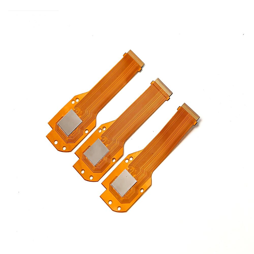
Via Covering Technology: Advanced PCB Protection for Enhanced Circuit Performance

All Categories

via covering

Via covering is an essential component in printed circuit board (PCB) manufacturing that serves to protect and insulate electrical connections. This specialized material is designed to cover via holes, which are the conductive pathways that connect different layers of a PCB. The covering prevents solder from flowing through the holes during the assembly process while maintaining electrical connectivity. Modern via coverings utilize advanced polymer compositions that offer excellent thermal stability and durability, capable of withstanding high-temperature soldering processes without degradation. These materials are engineered to provide reliable protection against environmental factors such as moisture, chemicals, and mechanical stress, ensuring the long-term reliability of the PCB assembly. Via coverings come in various forms, including liquid photo-imageable materials and film-based solutions, each offering specific advantages for different applications. The technology behind via covering has evolved to meet the demanding requirements of miniaturization in electronics, supporting higher density circuit designs while maintaining signal integrity.

New Products

Via covering technology offers numerous significant benefits for PCB manufacturers and end-users alike. The primary advantage lies in its ability to protect sensitive electronic components from contamination and environmental damage, significantly extending the lifespan of circuit boards. The covering material creates an effective barrier against moisture infiltration, preventing oxidation and corrosion of copper traces and other metallic components. This protection is particularly crucial in harsh operating environments where exposure to humidity, chemicals, or extreme temperatures is common. Additionally, via covering enhances the mechanical strength of the PCB assembly, providing better structural integrity during thermal cycling and mechanical stress. The material's excellent adhesion properties ensure long-term reliability, while its compatibility with various surface finishes allows for flexibility in manufacturing processes. Modern via coverings also contribute to improved signal integrity by reducing electromagnetic interference and cross-talk between adjacent circuits. The technology supports higher density designs by allowing for smaller via sizes and tighter spacing, enabling the development of more compact electronic devices. Furthermore, the use of via covering materials simplifies the PCB assembly process by preventing solder wicking and reducing defects in the final product.

Latest News

Why Choose PCB Solutions for Industrial Applications?

09

Oct

Why Choose PCB Solutions for Industrial Applications?

The Evolution of PCB Solutions in Modern Industrial Landscapes The industrial sector has witnessed a remarkable transformation with the integration of advanced PCB solutions into its core operations. From automated manufacturing facilities to sophist...
View More
What Problems Can Happen in PCB Circuit Boards and How to Solve Them?

09

Oct

What Problems Can Happen in PCB Circuit Boards and How to Solve Them?

Understanding Common PCB Circuit Board Issues and Their Solutions PCB circuit boards are the backbone of modern electronics, serving as the foundation for countless devices we use daily. From smartphones to industrial machinery, these intricate compo...
View More
How Are PCBs Manufactured? Key Steps and Processes Explained

09

Oct

How Are PCBs Manufactured? Key Steps and Processes Explained

Understanding the Complex Journey of Circuit Board Production PCB manufacturing has revolutionized the electronics industry, enabling the creation of increasingly sophisticated devices that power our modern world. From smartphones to medical equipmen...
View More
Why Choose Professional PCB Manufacturing Services?

09

Oct

Why Choose Professional PCB Manufacturing Services?

The Critical Role of Expert PCB Production in Modern Electronics In today's rapidly evolving electronics industry, the quality and reliability of printed circuit boards (PCBs) have become more crucial than ever. Professional PCB manufacturing service...
View More

Get a Free Quote

Our representative will contact you soon.
Email
Name
Company Name
Message
0/1000

via covering

Enhanced Protection and Reliability

Enhanced Protection and Reliability

Via covering technology represents a breakthrough in circuit board protection, offering unparalleled defense against environmental threats. The advanced polymer composition creates an impermeable barrier that shields sensitive electronic components from moisture, dust, and chemical contaminants. This protection is particularly crucial in maintaining the integrity of electrical connections across different PCB layers. The covering material's molecular structure is engineered to maintain its protective properties even under extreme temperature conditions, ensuring consistent performance throughout the product's lifecycle. This reliability enhancement translates directly to reduced maintenance requirements and longer operational life for electronic devices. The technology's ability to prevent oxidation and corrosion significantly reduces the risk of circuit failure, making it an essential feature for applications in challenging environments.
Manufacturing Process Optimization

Manufacturing Process Optimization

The implementation of via covering technology brings substantial improvements to the PCB manufacturing process. The material's precise application characteristics allow for automated processing, reducing production time and labor costs while maintaining consistent quality. The covering's compatibility with standard PCB manufacturing equipment ensures seamless integration into existing production lines. Its rapid curing properties minimize processing time, enabling higher throughput in manufacturing operations. The technology's ability to prevent solder wicking during assembly significantly reduces defect rates and rework requirements, leading to improved yield rates and cost efficiency. Furthermore, the material's stable chemical properties ensure consistent performance across different manufacturing batches, contributing to better quality control.
Design Flexibility and Miniaturization

Design Flexibility and Miniaturization

Via covering technology plays a crucial role in enabling advanced PCB designs by supporting miniaturization efforts. The material's excellent electrical insulation properties allow for reduced spacing between components without compromising signal integrity. This capability is essential for developing compact electronic devices while maintaining high performance standards. The technology supports various via sizes and configurations, providing designers with greater flexibility in circuit layout and routing options. The covering's ability to maintain stable electrical characteristics across different frequencies makes it suitable for high-speed digital applications. Additionally, its compatibility with different substrate materials and surface finishes expands the design possibilities for specialized applications.
Via Covering Technology: Advanced PCB Protection for Enhanced Circuit Performance

Get a Free Quote

Our representative will contact you soon.
Email
Name
Company Name
Message
0/1000