When designing a printed circuit board (PCB), the thickness of the PCB is one of the critical factors determining the success of a project. PCB thickness refers to the overall height of the board, encompassing all copper layers, substrate, prepreg, solder mask, and surface finish from the bottom layer to the top layer. Selecting the appropriate thickness is crucial for designing electronic products, so it is important to consider and test the suitable thickness for the application before proceeding with the design.
The following PCB thickness guide provides a comprehensive introduction to PCB thickness standards, factors affecting board thickness, the impact of PCB thickness on electrical, thermal, and mechanical performance, and how to choose the right thickness based on specific needs. Whether you require a standard PCB thickness for a double-layer board or are exploring custom thickness options for a multilayer board, this guide will ensure your project meets manufacturing, assembly, and application requirements.
PCB thickness refers to the overall thickness of the PCB board, encompassing all laminated layers. Understanding PCB thickness is one of the fundamental basics that every PCB designer and manufacturer must master.

Structural Integrity: Appropriate PCB thickness ensures the circuit board meets mechanical durability expectations. Thicker PCBs are less prone to bending or breaking, which is particularly critical for larger boards or those subjected to mechanical stress.
Electrical Performance: PCB thickness affects signal transmission and impedance control, especially in high-frequency or RF PCBs. The dielectric thickness between copper layers is crucial for controlled impedance lines.
Thermal Management: Thicker substrates and increased copper foil thickness enhance heat dissipation efficiency.
Manufacturing and Assembly: Standardized PCB thickness helps optimize manufacturing and assembly processes, ensuring compatibility and stability with connectors, soldering techniques, and enclosures.
Application Adaptability: In scenarios involving heavy connectors or high-current power applications, thicker PCB materials are often required.
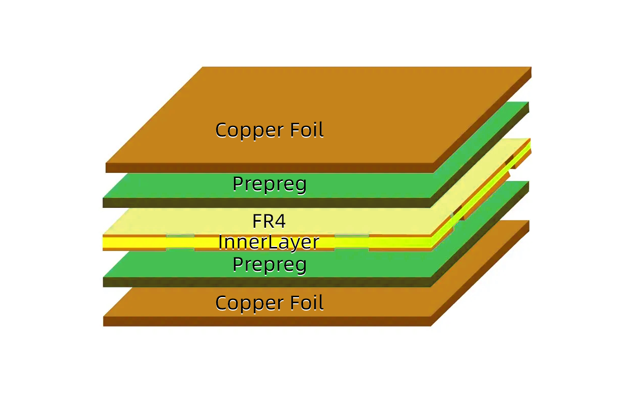
The overall thickness of a circuit board is the combined result of the thicknesses of all material layers in the design.
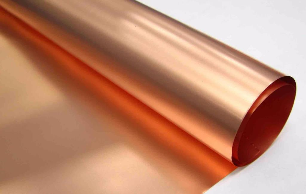
Copper Foil Layer:
Copper thickness is typically measured in ounces per square foot (oz). Standard copper thicknesses (such as 1oz, 2oz, and 3oz) directly impact the current-carrying capacity of traces and the thickness of the conductors.
Dielectric Core and Prepreg:
The selection of core materials (e.g., FR4, polyimide) and the thickness of the prepreg not only determine the overall thickness but also significantly influence electrical performance and thermal characteristics.
Solder Mask Thickness:
Although usually less than 0.05 mm, the presence of the solder mask slightly increases the overall thickness and plays a critical role in solder joint reliability.
Surface Finish Processes:
Whether it's ENIG (Electroless Nickel Immersion Gold), HASL (Hot Air Solder Leveling), or OSP (Organic Solderability Preservative), these processes add only micron-level thickness. However, they are crucial for solderability and hold particular significance in thickness control for fine-pitch or high-frequency applications.
Layer |
Typical Thickness (mm) |
Impact |
Copper Foil |
0.018–0.105 |
Current, signal integrity |
Prepreg |
0.06–0.20 |
Dielectric, bond layers |
Core (FR4) |
0.2–1.6 |
Board rigidity, insulation |
Solder Mask |
0.015–0.05 |
Protection, minimal thickness effect |
Surface Finish |
<0.01 |
Solderability, minimal thickness effect |
PCB Thickness (mm) |
Inches |
Standard Use |
0.4 |
0.016 |
Smart cards, flex PCBs, ultra-compact devices |
0.8 |
0.031 |
Compact consumer tech, IoT, wearables |
1.0 |
0.039 |
Mobile, general consumer, balanced designs |
1.6 |
0.063 |
Default for 2-layer PCB and most rigid PCBs |
2.0 – 2.4 |
0.079–0.094 |
Automotive, industrial control, robust boards |
3.2+ |
0.126+ |
Power/LED PCBs, thick high-power designs |
Copper foil thickness directly impacts signal processing and power handling capabilities, making it an indispensable core element in any PCB thickness guide.

Definition of Copper Thickness
Refers to the thickness of the copper layer on each side of the circuit board, typically measured in ounces per square foot (oz/ft²). For example, 1oz copper thickness is approximately 35 micrometers, which is the most commonly used benchmark unit in PCB manufacturing.
Core Impacts
Copper foil thickness not only determines the current-carrying capacity of traces but also directly affects the minimum trace spacing, overall board thickness, and thermal management efficiency.
Common Specifications and Applications
• 1oz (35µm) – Standard signal lines and power traces, widely used in consumer electronics.
• 2oz (70µm) – High-current and power PCBs, wider trace widths, enhanced thermal pathways.
• 3oz (105µm) – High-power circuits, LED drivers, and thick copper PCBs designed to withstand surge loads.
Copper Thickness |
μm |
Typical Use |
Effect on Board Thickness |
0.5oz |
18 |
Ultra-fine pitch, RF, HDI |
Minimal |
1oz |
35 |
General use, 2-layer PCB |
Most common thickness |
2oz |
70 |
Power, thermal, noise immunity |
Significant increase |
3oz+ |
105–210 |
Power, surge, heavy inverters |
Thickest, for specialty |
No guide to PCB thickness would be complete without an in-depth analysis of the key variables that determine the optimal thickness of a PCB. When selecting the appropriate thickness for your design, focus on the following critical elements:

PCB thickness directly impacts critical electrical and physical characteristics in the design.
Application |
Typical Thickness |
Why this Thickness? |
Smartwatches, IoT sensors |
0.6 – 1.0 mm |
Thin for compactness, light handling only |
Standard consumer (phones, tablets) |
1.0 – 1.6 mm |
Balanced for strength, signals, easy manufacture |
Power electronics, industrial boards |
2.0 – 2.4 mm |
High power, rugged, withstands heat/currents |
High-power LED lighting |
3.2 mm + |
Maximized heat dissipation, thick copper |
It is essential to clarify when custom or non-standard thicknesses are required.
Flexible and Wearable PCBs
• Require ultra-thin substrates (0.2–0.4mm) to maintain flexibility and comfort.
• Key guideline: Always verify the minimum bend radius and ensure the manufacturer can achieve precise thickness control without compromising strength.
High-Frequency and RF Circuits
• Precise impedance control demands strict dielectric layer thickness tolerances.
• Multilayer configurations should use specialized prepreg materials and minimize overall thickness for optimal signal fidelity.
High-Power/Industrial/Automotive Electronics
• Utilize robust thick cores (≥2.0mm) with heavy copper (2–3oz) to meet surge protection, thermal management, and safety requirements.
• Custom thickness may be necessary when using through-hole power connectors or large mounting screws.
LED Lighting and Power Modules
• Aluminum or ceramic substrates typically exceed 2mm in total thickness to ensure efficient heat dissipation from components.
• Thermal management becomes a core consideration in thickness design.
Here’s your straightforward guide to PCB thickness selection:

Define application and environment: Ask yourself: What mechanical, electrical, and thermal demands will my board face? This will determine the optimal thickness.
Choose a standard if possible: 1.6mm is the go-to for most designs, making PCB manufacturing cheaper and assembly smoother.
Calculate copper thickness requirements: Use IPC standards and calculators to determine minimum copper for your peak current.
Factor PCB layer count: More layers = added thickness. A multilayer PCB will always be thicker than a 2-layer PCB with identical core material.
Simulate stack-up: Use PCB design tools to visualize and validate your stack-up—some allow thickness sweeps to optimize for performance and manufacturability.
Consult your PCB manufacturer: Early feedback can help you balance performance with what’s easily buildable and avoid manufacturing roadblocks.
Document your requirements: Specifying thickness, copper weight, and dielectric stack-up in your fab notes minimizes miscommunication and helps ensure your PCB meets expectations.
Q: What is standard PCB thickness?
A: Standard PCB thickness is 1.6mm, but many values from 0.4mm to 3.2mm are supported.
Q: How is the overall board thickness specified?
A: Thickness refers to the total height from one surface of the PCB to the other, including all layers and finishes.
Q: Why is the thickness of a PCB board so important?
A: Thickness affects strength, signal performance, heat handling, and manufacturing compatibility.
Q: I have a 2-layer PCB—what’s the recommended thickness?
A: Most 2-layer boards use 1.6mm, considered best for mass-market connectors and handling.
Q: Can I request custom thickness for my PCB?
A: Yes, custom thickness is possible. However, non-standard thicknesses may require longer lead time and higher PCB production costs. Always communicate your custom thickness needs early with your PCB manufacturer.
Q: Does thickness of the PCB affect assembly?
A: Absolutely. Boards thinner than standard (e.g., less than 1.0mm) may require special handling during PCB assembly, while thickness above 2.4mm may not fit common automated assembly or connector systems without modification.
Q: Does increasing thickness improve reliability?
A: Not always. While a thicker PCB can increase mechanical strength and heat dissipation, unnecessary thickness may lead to increased material costs and make it harder to achieve fine features needed for high-density PCB design.
Q: Are there guidelines for choosing PCB copper thickness?
A: Yes! Consult IPC-2221 and your PCB manufacturer’s design guide for recommended copper thickness based on current-carrying needs; for most applications, 1oz or 2oz is used, but power designs may require 3oz or even higher.
Q: How does thickness of the copper affect etching and fabrication?
A: Increased copper foil thickness requires larger minimum trace width/spacing and can increase etching difficulty, especially in multilayer PCBs with high copper thickness on multiple layers.
Q: Is there an optimal thickness for all PCB designs?
A: No single size fits all. To determine the optimal thickness, analyze your mechanical, electrical, and cost requirements for each project. Use this comprehensive guide to inform your choice.
Understanding PCB thickness standards, the importance of copper thickness, and the factors affecting the overall board thickness is essential for modern PCB design and manufacturing. The right thickness of a PCB directly impacts every key aspect of your device: electrical performance, thermal management, mechanical robustness, manufacturability, and cost effectiveness.