Introduction
Smartphones, watches, televisions, and other electronic devices are ubiquitous in our daily lives, bringing countless conveniences. Their emergence is inseparable from the invention of printed circuit boards (PCBs). Printed circuit boards not only enable the miniaturization of electronic devices but also reduce the manufacturing costs of high-performance circuits. In this article, I will detail what PCBs are, their types and designs, and their importance to the development of modern technology.
What is a PCB?

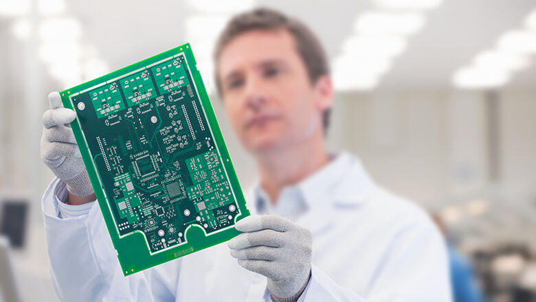
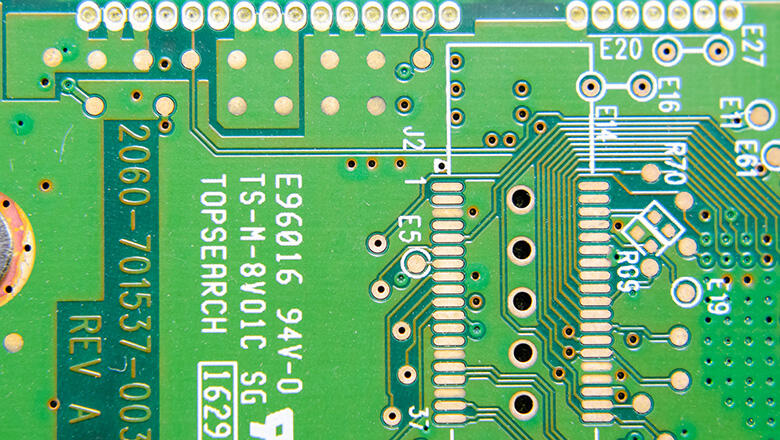
PCB is one of the core components of electronic devices. It is composed of multiple key parts, each with a specific function. PCB is used to connect and support electronic components and provide electrical and mechanical support.PCBs use conductive pathways, tracks or signal traces etched from copper sheets laminated onto a non-conductive substrate that does not conduct electricity. Electronic components are then added to the board and etchings are made on its surface, which allow the current to flow through the copper from component to component.
PCB Basics
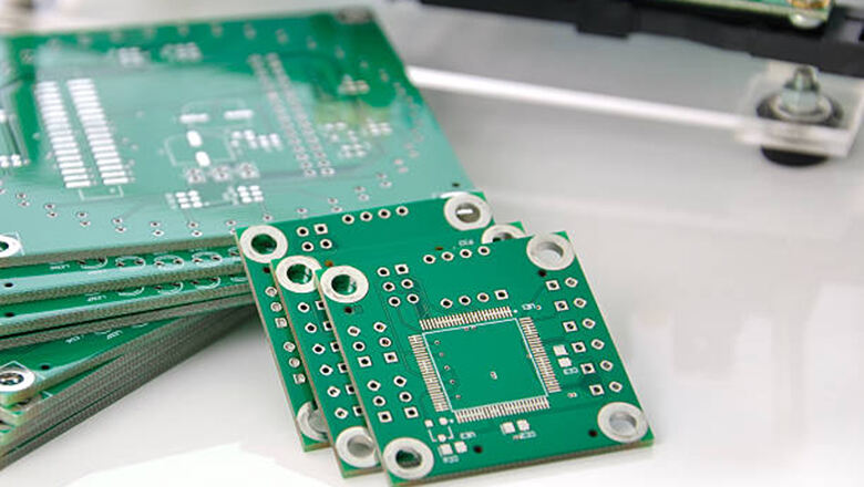
- Bare board: A bare board is ,also known as an unpopulated PCB, is a printed circuit board that carries no electronic components and cannot perform any electrical functions.
- Single-sided PCB: A single-sided PCB means that components and circuit traces are located exclusively on one side of the board.This type of PCB is simple and most used PCB because these PCBs are easy to design and manufacture.
- Double-sided PCB: Features copper traces are laminated on both sides of the substrate, supporting more complex circuit designs and utilizing vias (plated through-holes) to establish connections between layers. Compared to single-sided boards, it can accommodate more sophisticated circuits while maintaining excellent cost-effectiveness.
- Multilayer PCB: Multilayer PCB means that, this type of PCB has at least three conductive layers of copper. It is primarily achieved by laminating and bonding multiple PCB layers with insulating prepreg materials, resulting in higher circuit density and enabling the production of advanced circuit boards for computers, servers, and telecommunications equipment.
PCB Acts As
- The base of the pcb for every circuit design.
- A map for mounting components and routing signals.
- A platform to implement complex electronic device operations.
Types of Circuit Boards and PCB Layers
It is essential to understand different types of circuit boards is key for engineers, designers, and students entering the electronics industry.
Common Types & Structures
Type |
Description & Use |
Single-sided PCB |
One copper layer, all components on one side. Cost-efficient; used in simple devices and lighting. |
Double-sided PCB |
Copper layers on both sides for intermediate circuit complexity. Used in audio, test equipment, and some power supplies. |
Multilayer PCB |
4, 6, 8, or more layers sandwiched for compactness and performance. Vital for computers, medical, telecom, and automotive applications. |
Flex PCB |
Flexible substrate, allows bending (useful in wearable electronics, cameras, and foldable mobile devices). |
Rigid PCB |
Stiff, traditional design for most robust and durable applications. |
Rigid-Flex PCB |
Mixes rigid and flexible areas for intricate pcb design—beneficial in aerospace or advanced medical tools. |
HDI PCB |
High-Density Interconnect: “tightest” design, very fine traces, microvias; supports phones, tablets, and IoT. |
Materials and Structure in PCB Design

The layer stack-up and material selection of a PCB directly determines the reliability, performance, and production cost of electronic devices.
Essential Materials
- Copper Layer: It is the conductive backbone of a PCB ,typically made of copper foil, forming the signal transmission pathways on the circuit board.
- Insulating Material: Common substrate materials include FR-4 (fiberglass epoxy) for standard boards, polyimide for flexible circuits, and ceramic substrates for high-end military/medical equipment.
- Solder Mask: The colored coating (typically green) that cover the copper foil to protects the copper and to defines the surface of the pcb.
- Silkscreen: Prints identifiers and guides on the pcb surface facilitate component placement and system diagnostics.
PCB Layers and Board Layout
- Layer of a PCB: Layer of a PCB can be configured for signal, power, or grounding needs. The design rules and stack-ups directly affect signal speed, crosstalk, and EMI management.
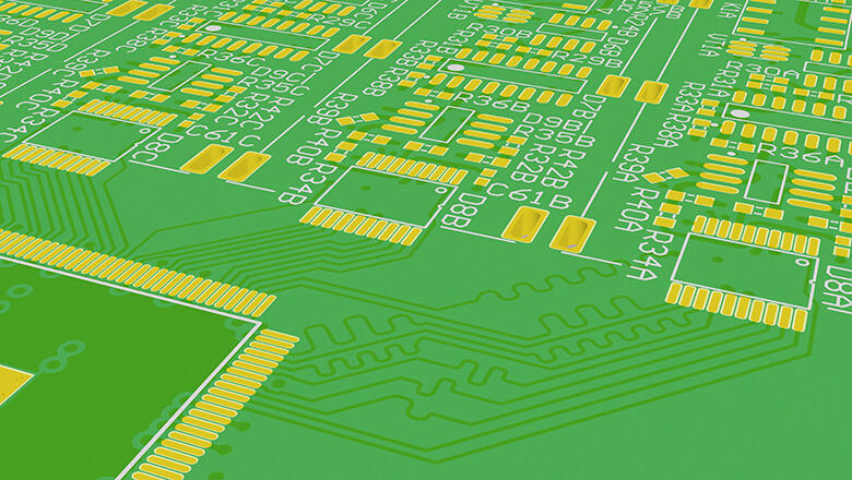
- PCB Traces: Circuit pattern is defined by thin and precise paths of copper. Their width and spacing play a crucial role in current capacity and signal behavior.
- Via: Plated holes that connect layers of the pcb and serve a vital function in double-sided and multilayer boards.
Simplified Comparison
Feature |
Single-sided |
Double-sided |
Multilayer |
Copper Layers |
1 |
2 |
3+ |
Component Density |
Low |
Medium |
High |
Design Complexity |
Basic |
Moderate |
Complex |
Example Use |
Flashlights |
Radios |
Smartphones |
How a PCB is Made & The Design Process

PCB Design Tools and Steps
Concept & Schematic
Define the circuit and select components. Popular pcb design tools such as Altium, Eagle, and KiCAD provide computer-aided design capabilities to ensure precise and error-free layouts.
Layout & Routing
Convert the schematic into PCB layout, arranging components and drawing connection traces. Key point is minimizing the trace length for critical signals.
Design Review & Simulation
Conduct Design Rule Checks (DRC) to minimize production risks; simulate signal flow to ensure no crosstalk or performance loss.
Gerber File Generation
Convert the design to industry-standard files for pcb production.
Fabrication
PCB is made by layering copper and insulating material, imaging the circuit, etching, drilling vias, applying solder mask, and then silkscreen.
Assembly
Components are mounted (SMT for surface-mount or THT for through-hole) and soldered onto the pcb.
Final boards are inspected, tested, and shipped.
Components on PCBs and How Circuits Work

Printed circuit boards (PCBs) cannot function independently, so each PCB is composed of a variety of electronic components, including not only basic passive devices such as resistors and capacitors, but also complex components such as integrated circuits, relays, sensors, and connectors. The placement of these components is highly flexible and can be arranged according to design requirements. They can be distributed individually on the top or bottom layers of the board, or they can be assembled collaboratively on both sides in double-sided or multi-layer board structure to jointly construct a fully functional circuit system.
- Traces and Vias: Allow signals to pass “across the board” and between layers in a compact, protected manner.
- ICs: Perform logic operations, data storage, and signal processing—foundation for smart modern electronics.
- Passive Elements: Provide filtering, timing, and power management.
- Active Components: Control switching, amplification, or data processing.
How Circuit Boards Work:
- Power is routed from a source through copper traces to each component, activating the circuit pattern as defined by the pcb design.
- Signal pathways are shielded/segregated by ground and power layers to ensure clean operation in complex circuit designs.

Applications and Advantages in Modern Electronics
Boards are used in nearly every field:
- Consumer Devices: Single-sided, double-sided, and high-density multilayer boards are employed in phones, laptops, smartwatches, and wearable devices.
- Industrial Electronics: Robust rigid PCB designs and occasionally flex circuits are required for robotics, control modules, sensors, and power supplies, particularly for moving joints.
- Medical Equipment: Multilayer, rigid-flex, or HDI PCBs with high reliability are often required in diagnostic machines and portable monitors.
- Automotive & Aerospace: Flexible, multilayer, or metal-core PCBs are utilized to withstand vibrations, harsh temperatures, and high electrical loads.
Major Advantages
- Achieve higher circuit densities for compact designs.
- Reduce costs through automated PCB production and assembly.
- Replace faulty boards easily with modular repair and upgrade.
- Protect copper layers and maintain circuit usability.
- Facilitate intricate, reliable, and faster circuit designs for modern requirements.
Future Trends and Tips in PCB Industry

As technology advances, the PCB industry continues to evolve.Here’s what’s shaping the next era of printed circuit board development and applications:
The Move Toward Higher Density and Miniaturization
- HDI Design: The growing demand for higher circuit density is driving the widespread adoption of High-Density Interconnect (HDI) PCBs.These are integral in smartphones, tablets, and advanced wearables, featuring microvias and ultra-fine traces to fit more connections in less space.
- Flexible Substrate & Flex PCB Innovations: The popularity of flexible circuits means more designs now require flex pcb or rigid-flex solutions, allowing electronic devices to bend, fold, and fit into previously impossible form factors—particularly critical for medical implants, foldable phones, and automotive sensors.
Advanced Materials and Environmental Focus
- New insulating materials and board substrates are continuously emerging, aiming to achieve lower transmission loss, enhanced thermal management efficiency, and more environmentally conscious manufacturing processes.
- Lead-free soldering, halogen-free laminates, and recyclable PCB production are being increasingly prioritized to meet global sustainability standards.
Smarter PCB Design and Testing
- Computer-Aided Design Tools: These enable rapid prototyping, error prediction, and simulation before physical boards are made, reducing costly rework while significantly shortening design cycles even for complex circuit boards.
- Design Review and Testing: Digital twin and circuit simulation technologies can precisely replicate real-world circuit behavior, identifying potential flaws at the design stage.
- Automated Optical Inspection (AOI): While a PCB is tested after production, AI-powered AOI and electrical testing catch micro-defects, ensuring production yields and reliability for mission-critical applications.
Conclusion
In essence, the PCB is like the invisible skeleton of all electronic devices. We don't often see it in our daily lives, but it's hidden within every product we use. It doesn't simply connect and secure electronic components. With its diverse types and precise designs, it adapts to the needs of different scenarios, making the possibilities of smart living a reality.
