All Categories
News
Home> News

How to Read PCB and Identify Components: The Complete Guide for Circuit Boards

2025-11-03

Introduction to Printed Circuit Boards and Circuit Analysis

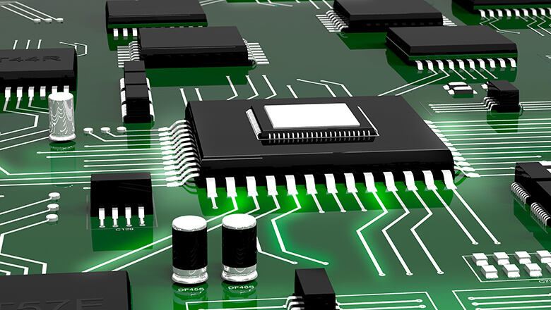
Printed circuit boards (PCBs) are the heart of modern electronic products; almost all devices rely on them. Different types of electronic components are arranged, interconnected, and mounted on PCBs, together forming the foundation of these devices.

A printed circuit board (PCB) is comparable to a detailed map. To learn how to interpret it, it's essential to understand not only the layout of the components but also the path of the traces that carry electrical signals and power. Regardless of your level of expertise in electronics, you must master three fundamental skills: component identification, PCB interpretation, and comprehensive electronic circuit analysis.

Why?

  • Helps you diagnose failures and perform repairs
  • Aids in optimizing designs for performance and durability
  • Allows you to modify or upgrade existing circuits
  • Enables you to reverse engineer or create documentation for legacy products

This guide will not only teach you how to identify each component, understand its electrical function, and read circuit diagrams, but also enable you to perform circuit analysis to understand how your electronic devices work.
electronic-components-pcb​.jpg

Macros of Printed Circuit: Anatomy, Layers, and Common Features

pcb.jpg

The macroscopic structure of a printed circuit board—its main architectural elements—determines the limitations and complexity of reading it. Whether examining a simple two-layer board or analyzing a high-speed multilayer design, understanding the following fundamental principles is crucial:

Layers of the PCB

A printed circuit board (PCB) can have anywhere from a single copper layer to dozens of layers—each layer serving a specific function of circuitry or power distribution.

Layer Name

Description

Function

Top Layer

The uppermost conductive layer

Where most components are placed (surface of the pcb)

Internal 1-N

Sandwiched copper planes and signal layers

Used to save space and carry electrical power/signals

Bottom Layer

The lowest conductive layer

Often used for routing or additional board space

Solder Mask

Polymer overlay for insulation

Prevents shorting during soldering, color-coded

Silkscreen

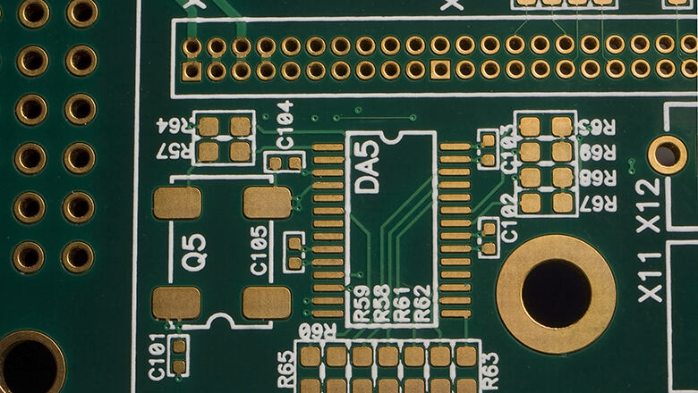
Printed legends and component designators

Helps identify components on the board easily

Modern electronic products typically use printed circuit boards with 4, 6, or even 12 or more layers to achieve high-density, high-speed.

Other Key Features in PCB Layout

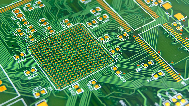
  • Vias: Vias are copper-plated holes that connect traces between layers,allowing components to communicate across different PCB layers.
  • Pads: Circular or rectangular copper areas for soldering component leads or SMD parts.
  • Traces: Thin copper lines (wires on the PCB) that carry signals and power. Width and routing impact circuit performance.
  • Component Footprints: Exact structures where specific components are placed and soldered.
  • Test Points: Small components or pads used to probe data signals between components during circuit testing and analysis.

Why Reading Circuit Boards and Identifying Components Matters

pcb-components​.jpg

Whether you're a PCB designer, a repair technician, or an electronics enthusiast, you can benefit from accurately interpreting circuit boards:
  • Diagnosing Issues: When equipment malfunctions, circuit board reading and component identification can accurately locate the problem area, thus saving a lot of troubleshooting time.
  • Design Feedback: Analyzing the interconnection between components on a circuit board can effectively uncover design flaws and identify optimization opportunities.
  • Upgrading and Modifying: If you want to swap a capacitor for better performance or add a filter, you must master the skill of interpreting the PCB component layout.
  • Component Sourcing and Procurement: Reading circuit boards helps create accurate bills of materials for manufacturing, repair, and maintenance.
  • Training New Technicians: A solid understanding of PCB structure and component identification is a core foundation for employees and students to delve into complex circuit design.

Understanding Circuit Diagrams, Schematic Symbols, and PCB Footprints

pcb-board-components​.jpg

Understanding circuit schematics is crucial for translating conceptual circuit designs into physical trace layouts on printed circuit boards.

Schematic Symbols and PCB Footprints

  • Schematic Diagram: Standard graphic symbols are used to represent circuit boards, components, and their electrical connections.
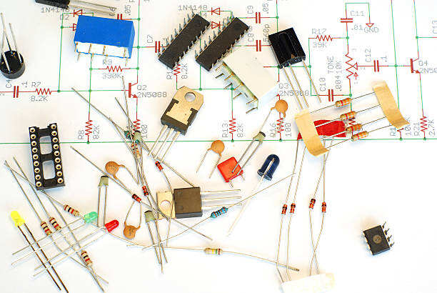
  • Component Designators: Unique letter-number codes (R13, C5, U2) simplify component lookup.
  • Footprints: The PCB version of a component’s schematic symbol—specifying where and how components are placed on the board.

Common Component Designators

Designator

Component

Electrical Function

R

Resistor

Limits current, divides voltages (Ohm’s Law)

C

Capacitor

Stores energy, filters, sets timing (Farads)

L

Inductor

Stores energy in magnetic field, filters

D

Diode

Allows current one way, ESD, rectification

Q

Transistor

Amplify or switch electronic signals

U or IC

Integrated Circuit

Multi-function, logic, op-amp, microcontroller

J

Connector/Jumper

Physical bridge for external/inter-board connections

F

Fuse

Overcurrent protection

T

Transformer

AC voltage/current conversion, isolation

Types of Components on the Board: Active, Passive, and More

components-of-pcb​.jpg

Passive Components

  • Resistors: Used to set currents/voltages per Ohm’s Law, bias transistor bases, pull-up/down logic lines.
  • Capacitors: Store energy (Farads), used for filtering, decoupling, and timing circuits; different types (ceramic, electrolytic, tantalum) suited for different signals.
  • Inductors: Store energy in magnetic fields, smooth current in power supplies (used in filters).

Active Components (continued)

  • Diodes: In complex circuit designs, diodes, in addition to rectification, can also perform various functions such as voltage regulation (Zener diodes), light emission (LEDs), and signal isolation.
  • Integrated Circuits (ICs): These integrated circuits integrate complete electronic circuits such as operational amplifiers, voltage regulators, microcontrollers, analog and digital processors, etc. onto a single chip. Each integrated circuit contains many electronic components interconnected in a very compact, miniature layout to perform signal amplification and switching functions.

Additional Component Categories

  • Connectors and Jumpers: It provides electrical and physical connections for a variety of PCBs or onboard points, enabling modularity, easy upgrades, and simplified testing.
  • Sensors and Electromechanical Devices: These devices include temperature, light, or pressure sensors, relays, and small electromechanical components such as motors and buzzers.
  • Protection and Filtering Components: Fuses, MOVs (metal oxide varistors), and ferrite beads are used to protect sensitive circuitry during surges and filter out EMI/RFI noise.

pcb.png

How to Read a PCB: Step-by-Step Process

The following describes how to systematically read PCB boards and identify components for circuit analysis and repair:

1. Survey the Surface of the PCB

First, visually inspect the surface of the printed circuit board. Look for:

  • The largest components (e.g., transformers, ICs, connectors).
  • Power input section (DC jack, battery contacts, or USB port).
  • Edge connectors and interface ports.

2. Locate Component Designators

Please note the silkscreen labels on the circuit board, such as R, C, L, Q, U, and D. These are component identifiers that correspond to your circuit diagram or bill of materials. This is the easiest way to identify each component and match it with its symbol on the circuit diagram.

3. Understand Circuit Sections

Most modern electronics organize the PCB into functional blocks. For example:

  • Power Supply Section: Rectification (diodes, bridge), filtering (capacitors), regulation (ICs, Zener diodes).
  • Microcontroller/Logic Section: ICs and support passives.
  • Input/Output Section: Connectors, switches, small components like filter caps and resistors.
  • RF/Analog Section: Components used for amplifiers, filters, antennas—often shielded for EMI.

4. Identify Key Traces and Vias

On multilayer or high-component-density printed circuit boards, traces may span the entire board or pass through internal layers. Vias are used to connect signal lines between layers, and careful examination (sometimes requiring a magnifying glass) can reveal how components are interconnected.

5. Check for Correct Orientation for Polarized Components

Always check for the correct orientation for polarized components:

  • Electrolytic and tantalum capacitors
  • Diodes (stripe = cathode)
  • LEDs (flat side or shorter lead = cathode)
  • ICs (pin 1 marked by a dot or notch)
  • Transformer dots denote winding polarity

A reversed polarized component can damage the circuit or degrade overall circuit performance.

Component Designators and Labels: How to Identify Each Component

Component identifiers are a core tool for deciphering circuit boards and accurately identifying each component.

Quick Reference Table for Designators:

Designator

Meaning

Additional Notes

R

Resistor

Fixed, variable (POT), thermistor, varistor

C

Capacitor

Electrolytic, ceramic, tantalum, trimmer

L / FB

Inductor / Ferrite

Filters, EMI, energy storage

D

Diode

Zener, LED, rectifier, photodiode, Schottky

Q

Transistor

BJT, FET, MOSFET, IGBT

U / IC

Integrated Circuit

Op-amps, microcontrollers, logic, memory

J / P

Connector, Jumper

Header, test points, sockets, interface

F

Fuse

Overcurrent protection

T

Transformer

Isolation, AC-AC conversion

Y

Crystal/Oscillator

Clock generation

SW

Switch

User/control input

Correct Orientation for Polarized Components

pcb-component​.jpg

Ensuring that all polarized components are oriented correctly is fundamental to the safe and reliable operation of any circuit:

  • Electrolytic Capacitors: ‘–’ (negative) lead is usually shorter and aligns with a stripe on the body, also indicated on the PCB silkscreen.
  • Diodes/LEDs: Stripe is the cathode; for SMD LEDs, a flat edge or dot often marks the cathode.
  • Tantalum Capacitors: Typically marked with a ‘+’ on the positive side.
  • ICs: Pin 1 is marked by a dot, indentation, or square pad; must match the PCB silkscreen.
  • Transformers: These dots are used to indicate the starting position of the windings. All winding connections must be made strictly according to the circuit diagram to avoid phase errors.

Neglecting proper orientation can result in immediate component failure or damage to the entire circuit.

Tips for Locating Specific Components Quickly

  • Use the Schematic and PCB Layout: Search for the component reference number in the schematic diagram and find its corresponding silkscreen label on the circuit board.
  • Highlighter Method: After printing the schematic, identify the actual components on the printed schematic while highlighting the confirmed components to avoid confusion.
  • Divide the PCB: The circuit board can be divided into physical or logical partitions according to its functions (power, signal, I/O, MCU, RF) to facilitate targeted troubleshooting.
  • Magnification: When inspecting small or densely packed PCBs, a magnifying lamp or microscope can be used to observe fine silkscreen or etched markings.
  • Continuity Testing: Use the continuity test mode of a multimeter to verify whether the connections of various components in a circuit are correct, or to trace hidden networks.

Components Used in Filters, Storage,Amplification, and Switching

  • Resistors and capacitors are widely used in various circuits and high-pin-count components, primarily for filtering and decoupling. For example, capacitors are often connected in parallel with the power supply to suppress voltage ripple by rapidly storing and releasing charge.
  • Inductors and capacitors are often used in pairs (forming LC circuits) as various functional elements in filters, oscillators, or radio frequency tuning circuits.
  • Transistors/ICs: This device is widely used in amplification and switching circuits, as well as in implementing logic operations and information storage in digital systems.
  • Transformers: Efficient for AC signal isolation or voltage step-up/down (especially in power and audio applications).
  • Diodes: This device is primarily used for DC, preventing reverse voltage connections, and establishing a reference voltage.
  • Switches and Relays: Used to save energy or data (momentarily or permanently change circuit state).

Advanced Reading: PCB Inspection, Design, and Analysis

PCB Inspection Techniques

Visual PCB Inspection:

  • Look for burnt, bulging, cracked, corroded, or discolored components.
  • Examine solder joints for cracks, bridges, or cold joints—rework as needed.

Functional Testing:

  • Measure voltages across suspected components directly on the board.
  • Use test points to probe specific signals, confirming operation or searching for faults.

X-ray, AOI, and ICT:

  • Quality inspection of high-density/multilayer PCBs requires specialized equipment such as AOI, X-ray, or ICT to detect hidden faults that are difficult to see with the naked eye.

Circuit Analysis: Interpreting Circuit Board Layouts

  • Follow the Signal Path: Start at the input, trace through filters, amplifiers, and out to the output.
  • Check Power Integrity: Confirm that each voltage rail reaches every relevant component.
  • Simulate If Unsure: Before hardware debugging, PCB design software can be used to perform simulation analysis on the theoretical design.

Design for Reliability

  • Component Placement: Place sensitive or high-frequency components close to relevant ICs (e.g., capacitors are used for decoupling right at power pins).
  • Thermal Management: Thermal vias or large-area copper foils are used to achieve uniform heat dissipation and extend component life.
  • EMI and Grounding: Keep high-speed circuits short and routed away from sensitive analog sections.

Frequently Asked Questions (FAQs) on How to Read a PCB

Q: Can I learn to read a PCB without formal education?

A: Of course! We recommend starting with the basic kit, learning through online resources, and practicing by disassembling old circuit boards.

Q: How do I read a circuit board if the schematic is missing?

A: Reverse engineer: note the designators, trace connections with a continuity meter, identify each component, and draw a reference circuit diagram accordingly.

Q: How do I replace small components on densely packed PCBs?

A: This operation requires fine-tipped tweezers, a precision temperature-controlled soldering iron (or a hot air desoldering station for surface mount components), and suitable lighting and amplification equipment. Before replacing any component, carefully verify the component number and mounting orientation. After soldering, the solder joints and surrounding circuitry must be carefully inspected to prevent the formation of solder bridges that could cause circuit malfunctions..

Q: What’s the best way to identify components when silk screening is faint or missing?

A: If a circuit diagram is available, refer to it first. If not, try to find and compare similar PCB versions or bills of materials (BOMs) for the same product family. When performing actual analysis, use a multimeter in continuity mode to trace the circuit path starting from a known reference point on the board. Also, pay attention to any identifiable layout patterns. Crystal oscillators are typically located near the microcontroller, while filter capacitors are concentrated around the power input ports. Also, look for standard PNP/NPN transistor packages. Additionally, online technical forums and open-source hardware projects that provide circuit diagrams are reliable resources for identifying unmarked test points on the board.

Q: How important is the physical layout of the PCB for circuit function?

A: It’s very important.These factors determine the interconnection between components, the paths of data and power signals, and whether the circuit achieves its design goals. Layer stack-up, trace width, component placement, and the use of vias all affect the complexity of circuit analysis, the electromagnetic interference immunity of devices, and their heat dissipation capabilities. All of these are key factors in modern electronic product design.

Q: Is it possible to test components like capacitors, resistors, and diodes directly on the board?

A: This is generally permissible, but circuit effects must be considered. If the resistor is connected in series or parallel with other components, the measured value may differ from the nominal value. Capacitors in filter circuits should be checked for short circuits; an LCR meter is recommended as it provides more accurate data. If diodes are used in voltage protection circuits, their forward and reverse characteristics should be tested separately using a multimeter in diode mode. If the measured values are abnormal, the test should be repeated with the circuit open.

Q: What do PCB designers mean by “components are placed with respect to data flow”?

A: When placing components, design engineers typically position them in their corresponding physical locations based on the circuit's input/output logic. This functional separation approach has three advantages: shorter signal traces, higher system performance, and easier troubleshooting because it allows for faster identification of the required components.

Conclusion: Why You Should Know How to Read a Printed Circuit Board

Learning to interpret circuit boards and identify components is the key to unlocking the door to electronics technology! Mastering this skill will make repairing equipment, optimizing functionality, and designing your own systems a breeze. Whether facing simple two-layer boards, complex multi-layer boards, or circuit systems assembled from discrete components, once you understand the correspondence between schematic symbols and physical packages, grasp the principles of polarized component mounting, and learn to use modern analytical tools, you will be able to confidently tackle various challenges in the electronics industry.

how to read pcb and identify components the complete guide for circuit boards-0

Get a Free Quote

Our representative will contact you soon.
Email
Name
Company Name
Message
0/1000