
In today's rapidly evolving electronics industry, optimized circuit board design has become the cornerstone of successful product development. As electronic devices become increasingly complex and compact, the importance of efficient PCB layouts cannot be overstated. Engineers and manufacturers worldwide are discovering that strategic design optimization not only improves performance but also significantly reduces costs and time-to-market. The systematic approach to PCB design optimization encompasses various technical aspects, from signal integrity and thermal management to component placement and routing strategies.
Enhanced Performance Through Strategic Design
Signal Integrity Improvements
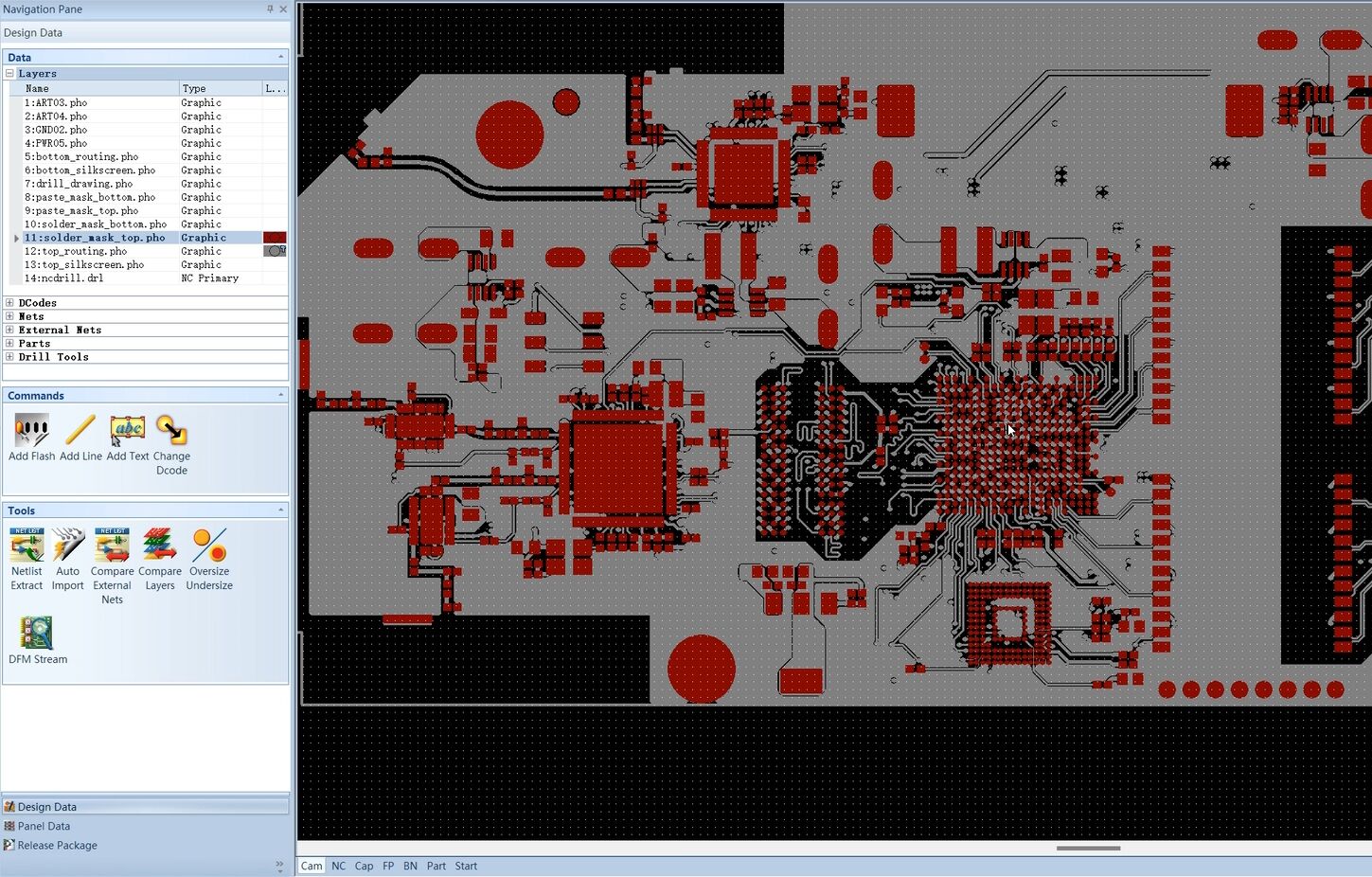
When implementing optimized circuit board design principles, signal integrity becomes dramatically enhanced through careful trace routing and impedance control. Engineers can minimize crosstalk between adjacent traces by maintaining proper spacing and implementing differential pair routing techniques. The strategic placement of ground planes and power planes creates a stable reference for high-speed signals, reducing electromagnetic interference and ensuring reliable data transmission. Advanced simulation tools allow designers to predict and mitigate potential signal integrity issues before manufacturing begins.
Modern PCB design software enables precise control over trace geometry, via placement, and layer stackup configuration. These tools help engineers maintain consistent impedance throughout the signal path, which is crucial for high-frequency applications. The optimization process includes careful consideration of trace width, dielectric materials, and copper thickness to achieve desired electrical characteristics. By addressing these factors early in the design phase, manufacturers can avoid costly redesigns and performance issues.
Thermal Management Excellence
Effective thermal management represents another critical benefit of optimized circuit board design methodologies. Strategic component placement ensures that heat-generating components are positioned to maximize heat dissipation while minimizing thermal coupling between sensitive circuits. Thermal vias and copper pours create efficient heat transfer paths, directing thermal energy away from critical components toward heat sinks or thermal pads.
Advanced thermal modeling software allows designers to simulate heat distribution patterns across the PCB before prototype development. This predictive capability enables engineers to identify potential hot spots and implement cooling solutions proactively. The integration of thermal considerations into the initial design phase prevents performance degradation and extends component lifespan, ultimately improving product reliability and customer satisfaction.
Cost Reduction and Manufacturing Efficiency
Material Optimization Strategies
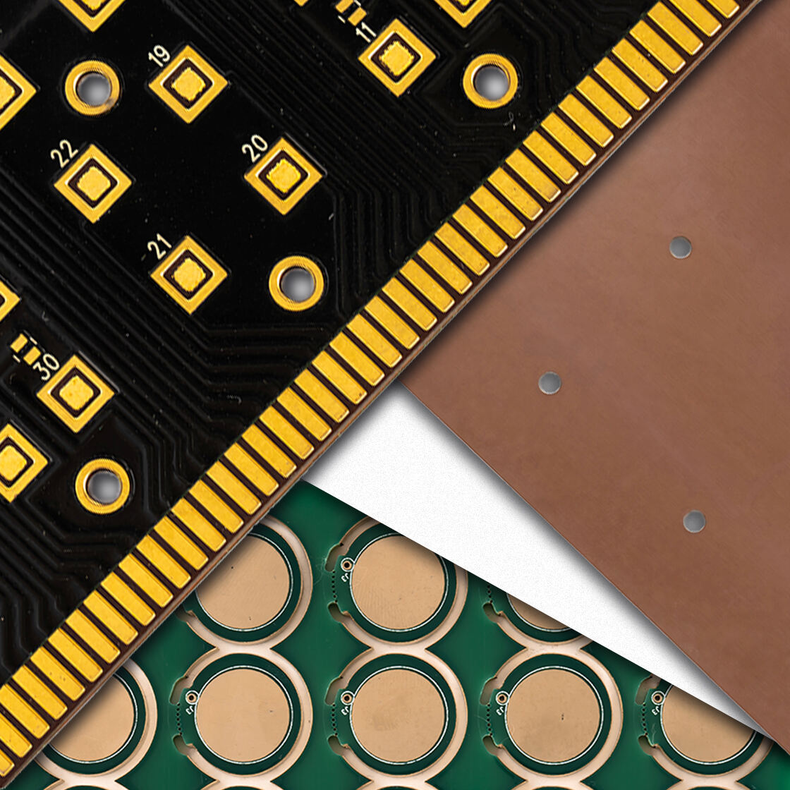
Optimized circuit board design significantly reduces material costs through intelligent layer count management and efficient space utilization. By carefully planning component placement and routing strategies, engineers can often reduce the number of PCB layers required while maintaining electrical performance. This reduction in layer count directly translates to lower material costs and simplified manufacturing processes.
Strategic panelization techniques maximize the number of boards that can be manufactured from a single panel, reducing waste and improving material utilization efficiency. Design optimization also considers standard PCB sizes and manufacturing constraints, ensuring compatibility with automated assembly equipment and reducing setup costs. The selection of appropriate via types and sizes minimizes drilling time and reduces manufacturing complexity.
Assembly Process Improvements
Manufacturing efficiency gains substantial improvement through optimized circuit board design practices that consider assembly requirements from the initial concept phase. Component placement optimization reduces pick-and-place machine travel time, decreasing assembly duration and associated labor costs. Standardized component orientations and consistent spacing simplify programming requirements for automated equipment.
Design for manufacturability principles ensure that all components can be accessed easily during assembly and testing procedures. Proper clearance around components facilitates automated optical inspection and reduces the likelihood of assembly errors. The optimization process includes consideration of solder paste application, reflow profiles, and wave soldering requirements to minimize defects and rework costs.
Reliability and Long-term Performance Benefits
Component Stress Reduction
Optimized circuit board design methodologies significantly reduce mechanical and electrical stress on components, leading to improved long-term reliability. Careful consideration of thermal expansion coefficients between different materials prevents solder joint failures due to thermal cycling. Strategic placement of components minimizes mechanical stress during handling and operation, reducing the risk of component damage or detachment.
Advanced finite element analysis tools enable designers to simulate mechanical stress patterns under various operating conditions. This predictive capability allows engineers to identify potential failure points and implement design modifications to improve durability. The optimization process includes consideration of vibration resistance, shock tolerance, and environmental factors that may affect component performance over time.
Enhanced Electromagnetic Compatibility
Electromagnetic compatibility improvements represent a crucial advantage of optimized circuit board design approaches. Proper grounding strategies and shielding techniques minimize electromagnetic emissions while improving immunity to external interference. Strategic placement of bypass capacitors and ferrite beads helps suppress high-frequency noise and maintain stable power delivery to sensitive circuits.
Careful routing of power and ground connections creates low-impedance current return paths, reducing electromagnetic radiation. The optimization process includes consideration of trace geometry, via placement, and layer stackup configuration to minimize loop areas and control electromagnetic fields. These design practices help ensure compliance with regulatory requirements and prevent interference with other electronic systems.
Design Flexibility and Future-Proofing
Modular Design Approaches
Modern optimized circuit board design strategies incorporate modular approaches that facilitate future upgrades and modifications. By designing functional blocks as discrete modules, engineers can update specific portions of the circuit without requiring complete redesigns. This modular methodology reduces development time for product variants and enables rapid prototyping of new features.
Standardized interface connections between modules simplify integration and testing procedures. The optimization process includes consideration of signal integrity across module boundaries and power distribution requirements. Modular design approaches also facilitate parallel development efforts, allowing different engineering teams to work simultaneously on separate functional blocks.
Scalability Considerations
Scalability planning within optimized circuit board design enables efficient adaptation to different product requirements and market demands. Flexible power distribution networks accommodate various component configurations and power consumption levels. Reserved space allocation and standardized connector placement facilitate future expansion without major layout modifications.
The optimization process includes consideration of component availability and lifecycle management to ensure long-term manufacturability. Design documentation standards and version control systems maintain design integrity throughout product evolution. These practices enable manufacturers to respond quickly to market changes while maintaining design quality and reliability standards.
FAQ
How does optimized circuit board design impact product development timelines
Optimized circuit board design significantly accelerates product development timelines by reducing the number of design iterations required. When engineers implement proper design practices from the beginning, they encounter fewer issues during prototyping and testing phases. Advanced simulation tools enable virtual validation of designs before physical prototypes are built, identifying potential problems early in the development cycle. This proactive approach minimizes costly redesigns and helps teams meet aggressive time-to-market goals while maintaining product quality standards.
What are the most critical factors to consider in PCB optimization
The most critical factors in PCB optimization include signal integrity management, thermal performance, electromagnetic compatibility, and manufacturing constraints. Engineers must balance electrical performance requirements with physical design limitations while considering cost targets and reliability goals. Component placement strategy affects multiple aspects of design performance, making it essential to optimize placement early in the design process. Power distribution network design and grounding strategies significantly impact overall system performance and should be carefully planned from the initial concept phase.
How does design optimization affect manufacturing yield rates
Design optimization dramatically improves manufacturing yield rates by reducing assembly defects and improving process repeatability. When designs consider manufacturing constraints and capabilities, they experience fewer issues during production runs. Proper component spacing, standardized orientations, and appropriate pad sizes facilitate reliable automated assembly processes. Design for testability principles enable comprehensive quality control procedures that catch defects early in the manufacturing process, reducing overall production costs and improving customer satisfaction.
What role does simulation software play in circuit board optimization
Simulation software plays a crucial role in circuit board optimization by enabling virtual validation of design concepts before physical implementation. Electromagnetic simulation tools help engineers predict signal integrity performance and identify potential interference issues. Thermal simulation capabilities allow designers to optimize heat management strategies and prevent thermal-related failures. Mechanical simulation tools validate structural integrity and help optimize component placement for reliability. These simulation capabilities reduce development costs and accelerate time-to-market by identifying issues early in the design phase.