
The electronics industry continues to evolve at an unprecedented pace, driving demand for more sophisticated and reliable printed circuit boards. Advanced PCB manufacturing has emerged as a critical differentiator for companies seeking to develop cutting-edge electronic products that meet stringent performance requirements. This technological advancement encompasses innovative fabrication techniques, enhanced material science, and precision engineering processes that deliver superior performance characteristics compared to traditional manufacturing approaches.
Modern electronic devices require circuit boards that can handle higher frequencies, support miniaturization efforts, and maintain reliability under extreme operating conditions. These demanding requirements have pushed manufacturers to develop sophisticated production methodologies that leverage state-of-the-art equipment, advanced substrate materials, and precise quality control systems. The result is a new generation of PCBs that enable breakthrough innovations across industries ranging from aerospace and medical devices to consumer electronics and automotive systems.
Enhanced Precision and Miniaturization Capabilities
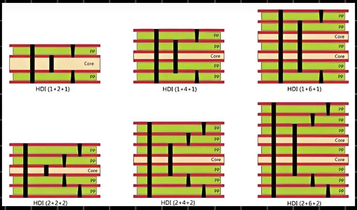
Micro-Via Technology and High-Density Interconnects
Advanced PCB manufacturing techniques enable the creation of micro-vias with diameters as small as 50 micrometers, facilitating unprecedented circuit density and component miniaturization. These microscopic connections allow designers to route signals through multiple layers with minimal space requirements, enabling the development of compact electronic devices without compromising functionality. The precision drilling and plating processes required for micro-via fabrication represent significant technological achievements that directly translate into smaller, more powerful electronic products.
High-density interconnect technology builds upon micro-via capabilities to create circuit boards with exceptional routing density and reduced layer counts. This approach enables manufacturers to pack more functionality into smaller form factors while maintaining signal integrity and thermal management characteristics. The resulting PCBs support complex electronic systems that would be impossible to implement using conventional manufacturing techniques, opening new possibilities for product designers and engineers.
Fine-Pitch Component Support
Modern electronic components continue to shrink in size while increasing in complexity, requiring PCBs that can accommodate fine-pitch packages with lead spacing as narrow as 0.3 millimeters. advanced PCB manufacturing processes incorporate specialized surface preparation techniques and precision solder mask application to ensure reliable connections with these demanding components. The ability to support fine-pitch packages directly impacts product performance and reliability, particularly in applications where space constraints are critical.
Surface mount technology optimization plays a crucial role in accommodating fine-pitch components, requiring precise pad geometries and controlled surface finishes. Advanced manufacturing processes ensure that solder paste application, component placement, and reflow profiles are optimized for each specific package type, resulting in consistent joint formation and long-term reliability. These capabilities enable the integration of the latest semiconductor devices and passive components into next-generation electronic products.
Superior Material Properties and Performance
Advanced Substrate Materials
The selection and application of advanced substrate materials represent fundamental advantages of modern PCB manufacturing processes. High-performance laminates incorporating PTFE, polyimide, and specialized ceramic fillers provide exceptional electrical properties, thermal stability, and mechanical strength compared to traditional FR-4 materials. These advanced substrates enable PCBs to operate reliably at higher frequencies, elevated temperatures, and challenging environmental conditions while maintaining consistent performance characteristics throughout their operational lifetime.
Low-loss dielectric materials have become increasingly important for high-frequency applications, where signal integrity and power efficiency are paramount concerns. Advanced PCB manufacturing incorporates these specialized materials through controlled lamination processes that ensure uniform dielectric properties and minimize signal degradation. The resulting circuit boards enable the development of high-performance RF systems, high-speed digital circuits, and power electronics that would be compromised by conventional substrate materials.
Enhanced Copper Technology
Advanced copper foil technology and specialized plating processes contribute significantly to PCB performance improvements, particularly in terms of current-carrying capacity and thermal management. Heavy copper PCBs, featuring conductor thicknesses exceeding 3 ounces per square foot, enable the handling of high current loads while providing excellent heat dissipation characteristics. These capabilities are essential for power electronics, automotive applications, and industrial control systems where thermal management and electrical performance are critical success factors.
Embedded copper coin technology represents another advancement that enables localized thermal management and current handling improvements without increasing overall board thickness. This approach allows designers to optimize conductor properties in specific areas while maintaining cost-effectiveness across the entire PCB design. The selective application of enhanced copper features demonstrates the flexibility and precision achievable through advanced manufacturing processes.
Improved Signal Integrity and Electrical Performance
Controlled Impedance Manufacturing
Precise impedance control has become a defining characteristic of advanced PCB manufacturing, enabling the consistent transmission of high-speed digital signals without degradation or interference. Sophisticated manufacturing processes incorporate real-time monitoring and adjustment systems that ensure trace geometries and dielectric properties meet stringent impedance specifications throughout the production process. This level of control is essential for maintaining signal quality in high-performance computing, telecommunications, and data processing applications.
Differential pair routing and controlled spacing techniques further enhance signal integrity by minimizing crosstalk and electromagnetic interference between adjacent conductors. Advanced PCB manufacturing processes ensure that these critical geometric relationships are maintained with exceptional precision, enabling the reliable transmission of high-speed differential signals used in modern digital communication protocols. The resulting PCBs support data rates that would be unachievable using conventional manufacturing approaches.
Advanced Via Technology
Blind and buried via technology enables complex multilayer designs while maintaining signal integrity and minimizing electromagnetic interference. These specialized interconnection methods allow signals to transition between specific layers without creating unnecessary discontinuities or parasitic effects that could compromise electrical performance. Advanced PCB manufacturing processes incorporate precise drilling, cleaning, and plating sequences that ensure reliable via formation and consistent electrical characteristics across all interconnections.
Via-in-pad technology represents another advancement that enables higher routing density while maintaining signal quality, particularly important for fine-pitch BGA packages and high-density connector interfaces. This approach requires specialized manufacturing processes to ensure that via fills and surface finishes meet the demanding requirements of direct component mounting. The resulting PCBs enable more compact designs while maintaining the electrical performance characteristics required for high-speed applications.
Enhanced Reliability and Quality Assurance
Advanced Testing and Inspection Methods
Automated optical inspection systems and advanced testing methodologies ensure that every PCB meets stringent quality standards before shipment to customers. These sophisticated quality control systems can detect microscopic defects, dimensional variations, and electrical anomalies that might compromise product reliability or performance. The implementation of comprehensive testing protocols throughout the manufacturing process enables the early detection and correction of potential issues, resulting in consistently high-quality products.
In-circuit testing and boundary scan techniques provide comprehensive electrical verification of complex multilayer PCBs, ensuring that all connections function correctly and meet specified performance criteria. Advanced PCB manufacturing facilities incorporate automated test equipment that can rapidly verify thousands of individual connections and components, providing detailed feedback on electrical performance and identifying any deviations from design specifications. This thorough testing approach minimizes the risk of field failures and ensures long-term product reliability.
Statistical Process Control
Implementation of statistical process control methodologies enables continuous monitoring and improvement of manufacturing processes, ensuring consistent quality and performance across all production runs. Advanced PCB manufacturing facilities collect and analyze thousands of data points throughout the production process, identifying trends and variations that could impact product quality. This proactive approach to quality management enables rapid response to process variations and continuous improvement of manufacturing capabilities.
Traceability systems integrated throughout the manufacturing process provide complete documentation of materials, processes, and test results for every PCB produced. This comprehensive record-keeping enables rapid identification of root causes when issues occur and facilitates continuous improvement initiatives. The ability to trace every aspect of the manufacturing process contributes significantly to overall product reliability and customer confidence.
Cost-Effectiveness and Manufacturing Efficiency
Optimized Production Processes
Advanced PCB manufacturing incorporates lean manufacturing principles and automation technologies that significantly reduce production costs while improving quality and consistency. Automated material handling systems, computer-controlled processing equipment, and integrated quality monitoring reduce labor requirements and minimize the potential for human error. These efficiency improvements enable manufacturers to offer competitive pricing while maintaining the high quality standards required for advanced PCB applications.
Optimized panelization strategies and advanced nesting algorithms maximize material utilization and reduce waste throughout the production process. These techniques ensure that raw materials are used efficiently while maintaining the spacing and orientation requirements necessary for reliable processing. The resulting cost savings can be substantial, particularly for high-volume production runs where material efficiency directly impacts overall project economics.
Reduced Time-to-Market
Streamlined manufacturing processes and advanced planning systems enable faster turnaround times without compromising quality or reliability. Advanced PCB manufacturing facilities utilize sophisticated scheduling algorithms and real-time production monitoring to optimize workflow and minimize processing delays. This capability is particularly valuable for companies developing time-sensitive products or responding to rapidly changing market demands where quick delivery can provide significant competitive advantages.
Design for manufacturing principles integrated into the development process help identify potential production issues early in the design cycle, reducing the need for costly revisions and delays. Advanced PCB manufacturers work closely with customers to optimize designs for manufacturability while maintaining performance requirements, resulting in smoother production processes and faster delivery times. This collaborative approach contributes to overall project success and customer satisfaction.
Environmental Sustainability and Compliance
Green Manufacturing Practices
Modern advanced PCB manufacturing incorporates environmentally responsible processes that minimize waste generation and reduce the environmental impact of production activities. Closed-loop chemical recycling systems, water treatment facilities, and waste reduction initiatives demonstrate the industry commitment to sustainable manufacturing practices. These environmental improvements not only reduce operational costs but also help customers meet their own sustainability objectives and regulatory requirements.
Lead-free soldering processes and RoHS-compliant materials have become standard elements of advanced PCB manufacturing, ensuring that products meet international environmental regulations without compromising performance or reliability. The transition to environmentally friendly materials and processes required significant investment in new equipment and process development, but the resulting products meet the stringent requirements of global markets while supporting environmental protection initiatives.
Regulatory Compliance
Advanced PCB manufacturing facilities maintain compliance with numerous international standards and regulations, including ISO 9001, ISO 14001, and industry-specific requirements such as IPC standards and military specifications. This comprehensive approach to quality management and regulatory compliance ensures that products meet the demanding requirements of diverse industries and applications. Maintaining multiple certifications demonstrates the manufacturer commitment to quality and provides customers with confidence in product reliability and consistency.
Documentation and certification processes integrated throughout manufacturing ensure that every product meets applicable regulatory requirements and industry standards. Advanced PCB manufacturers maintain detailed records of compliance testing, material certifications, and process validations that support customer qualification requirements and regulatory audits. This thorough approach to compliance management reduces customer risk and facilitates product acceptance in regulated industries.
FAQ
What makes advanced PCB manufacturing different from traditional methods
Advanced PCB manufacturing incorporates sophisticated equipment, precision processes, and advanced materials that enable higher performance characteristics compared to traditional methods. Key differences include micro-via technology, controlled impedance manufacturing, advanced substrate materials, and comprehensive quality control systems that ensure consistent performance and reliability.
How does advanced PCB manufacturing improve product reliability
Advanced manufacturing processes incorporate multiple quality control checkpoints, sophisticated testing methodologies, and statistical process control systems that identify and correct potential issues before they impact product performance. The use of high-quality materials and precision manufacturing techniques results in PCBs that demonstrate superior long-term reliability and consistent performance characteristics.
What types of applications benefit most from advanced PCB manufacturing
High-frequency RF applications, high-speed digital systems, power electronics, medical devices, aerospace systems, and automotive electronics benefit significantly from advanced PCB manufacturing capabilities. These applications require superior electrical performance, miniaturization, thermal management, and reliability characteristics that are achievable only through advanced manufacturing processes.
How does advanced PCB manufacturing support miniaturization efforts
Advanced manufacturing enables micro-via technology, high-density interconnects, fine-pitch component support, and optimized layer stackups that allow more functionality to be packed into smaller form factors. These capabilities enable the development of compact electronic devices without compromising performance or reliability, supporting the ongoing trend toward miniaturization across multiple industries.