Amid the ongoing innovation in the electronics industry, the inspection process remains the core support of the quality control system. Electronic engineers are responsible for monitoring product quality. Quality managers must oversee the production workflow. Circuit board contract manufacturers need to manage the final output. All relevant stakeholders must regard ensuring the superior performance of printed circuit boards as their primary responsibility. Contemporary circuit board designs are evolving toward greater complexity. High-density assembly technologies demand precise process control. Advanced design specifications continue to drive higher manufacturing accuracy. These technological advancements pose new challenges for inspection capabilities. Traditional inspection methods exhibit noticeable detection limitations. They struggle to effectively identify soldering defects located beneath components. These microscopic defects may also reside deep within the internal structures of components.
X-ray inspection technology demonstrates its distinctive value precisely at this stage. The technology achieves non-destructive internal detection, provides high-resolution detailed images, and accurately displays the internal structure of printed circuit boards. It must be acknowledged that X-ray inspection has evolved into an indispensable core testing technology. All manufacturers dedicated to producing high-quality circuit boards and electronic products need to depend on this technology to satisfy the industry's most stringent standards.

This in-depth guide aims to systematically elucidate the fundamental working principles of X-ray inspection technology. It will elaborate on the critical role this technology plays in quality control systems and introduce the primary inspection techniques widely adopted in modern industrial production. Furthermore, we will analyze the core functional features that contemporary X-ray inspection equipment should possess. The book also provides practical operational methods for obtaining high-value inspection images. Such images can clearly reveal various concealed defects that conventional inspection methods often fail to detect.
The electronics industry consistently demands stable product quality, accelerated production cycles, and highly reliable equipment. These stringent requirements have fundamentally reshaped the traditional role of quality inspection. Modern manufacturing systems have deeply embedded quality inspection into every essential stage of printed circuit board production.

Relying solely on traditional inspection methods leads to multiple issues. This approach allows certain internal defects to go undetected. It also results in a gradual decline in the overall reliability of printed circuit boards. Ultimately, these hidden risks manifest as functional failures during actual product use. X-ray inspection technology provides key technical support to address these challenges. This technology has become an indispensable core inspection solution for modern electronic product testing and manufacturing process validation.
Before we dive deeper into X-ray inspection technology, let’s see how it compares to classic inspection tasks:
Inspection Method |
Can Detect Hidden Defects? |
Speed |
Cost per Board |
Best For |
Visual Inspection |
✖ |
Fast |
Low |
Basic errors, low-volume production |
Automated Optical Inspection (AOI) |
✖ |
Very Fast |
Low-Medium |
Surface-mount, solder bridges, missing/shifted parts |
Flying Probe Testing |
✖ (mostly surface) |
Slow |
High (prototyping) |
Opens/shorts in circuit traces, net-level testing |
X-ray Inspection / AXI |
✔ |
Fast-Moderate |
Medium-High |
Internal layer analysis, BGAs, solder joint defect, complex PCBs |

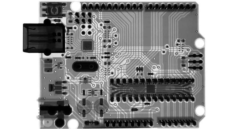
X-ray inspection is a testing method that uses X-ray radiation to generate energy waves that penetrate a PCB assembly. The difference in atomic weight between metals (like solder or copper) and organic materials (FR-4, resin) creates visible contrast on the x-ray image.
The selection of appropriate X-ray inspection methods by corporate decision-makers constitutes a comprehensive evaluation process. This process requires simultaneous consideration of specific inspection objectives, the physical characteristics of circuit boards, and the practical requirements of production lines.
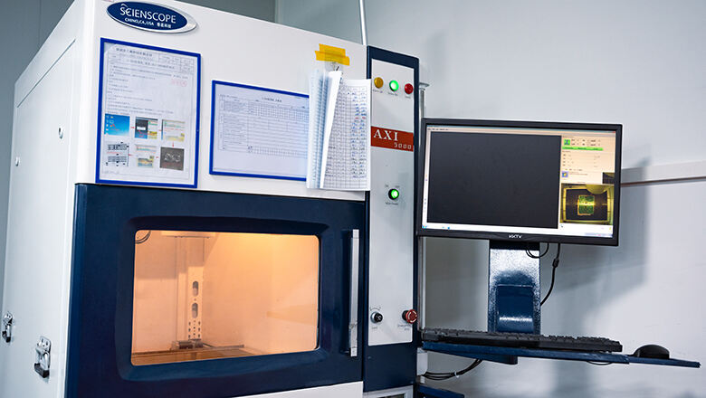
The advent of automated X-ray inspection (AXI) systems has revolutionized the printed circuit board manufacturing industry. By delivering reliable and high-efficiency inspection on every production line, these systems are driving its technological advancement. Advanced systems employ robotics to achieve full automation of the inspection process, encompassing board handling, scan imaging, and defect classification. These systems can consistently deliver rapid and stable inspection results with minimal human intervention.
Automated X-ray inspection systems employ sophisticated algorithms to perform real-time analysis of captured X-ray images.
These systems can automatically identify various typical defects, including solder voids, component misalignments, open circuits, and hidden bridges beneath BGA packages and other critical areas. By integrating AXI systems into quality management platforms, factories can achieve centralized archiving of all X-ray inspection data. This integrated solution comprehensively records defect trend analysis data and corresponding corrective actions, establishing a closed-loop quality management system.
Key highlights of AXI:
An effective x-ray inspection machine for pcbs and pcb assemblies will include the following:

One of the strongest arguments for using x-ray inspection in pcb quality control is its ability to reveal manufacturing issues that other inspection technologies simply can't see. Here’s what robust x-ray inspection capabilities can detect:
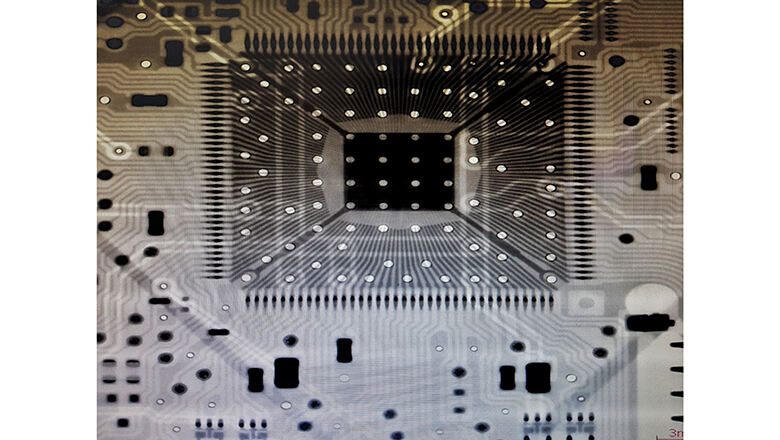
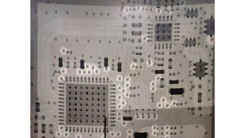
Solder Voids and Insufficient Solder: During the reflow soldering process, voids form within solder joints. This phenomenon compromises both the electrical connectivity and mechanical strength of the connections. Conventional inspection methods cannot detect these internal defects. X-ray inspection technology provides clear visualization of the complete internal structure.
Solder Bridges/Shorts: Especially under BGAs—where optical or probe-based methods fail—x-ray images reveal connectivity issues that can cause catastrophic field failures.
Misaligned Components: Accurately detects misplaced or skewed components, lifted leads, and tombstoning.
Open Circuits/Internal Cracks: Hidden cracks between inner layers or along traces from mechanical or thermal stress.
Filled/Buried Vias and Pinholes: This technology effectively identifies vias with voids or incomplete fillings, proving particularly critical for high-density interconnect boards and products utilizing via-in-pad designs.
Delamination and Layer Separations: Layered views obtained through 3D/CT X-ray imaging technology can clearly reveal delamination or separation between the layers of printed circuit boards. This method quickly identifies interlayer separation issues that are difficult to detect with conventional methods.
Capturing high-quality x-ray images is fundamental for reliable defect detection. Modern systems provide features such as automatic exposure control, programmable scan paths, and adjustable focus to suit specific pcb assemblies and component types.
Best practices for capturing x-ray images:
Automated x-ray inspection provides unique benefits that other testing and inspection methods cannot equal:
Benefit |
Description |
Hidden Defect Detection |
Uncovers defects below BGAs, inside vias, and within PCB layers |
Automation & Throughput |
Enables quality control and inspection at high speeds for every assembly |
Traceability |
Captures, stores, and links x-ray images to every serial/batch automatically |
Consistent Quality |
Reduces human error; every board inspected to the same stringent standards |
Complies with Quality Standards |
Supports robust audits and continuous improvement projects |
Cost Reduction |
Catches costly failures early, reduces warranty returns, and boosts customer trust |
Tips for maximizing these benefits:
Your choice will shape the reliability of your final product and the efficiency of your pcb manufacturing workflow.
Ask your x-ray inspection services provider:
Q: Why is X-ray inspection considered critical for quality in PCB assemblies?
A: X-ray inspection can see through layers and components, identifying hidden problems—such as voids, shorts, and misalignments—ensuring your circuit boards meet the highest industry standards that traditional inspection methods miss.
Q: What types of defects can only be detected using PCB X-ray inspection?
A: Defects like solder voids under BGAs, delamination between PCB layers, filled vias with internal voids, micro-cracks in traces, and subtle misalignment beneath large components are only visible to x-ray inspection technologies.
Q: Is x-ray inspection safe for my PCBs and for operators?
A: Yes—modern x-ray inspection machines are thoroughly shielded, and operators follow strict radiation safety guidelines. Proper settings keep both components and people protected.
Q: How does X-ray inspection improve inspection speed and quality?
A: Automated x-ray inspection systems capture high-resolution images and analyze them within seconds, providing consistent quality checks and reducing bottlenecks compared to slower manual methods.
Q: Do I always need 3D x-ray, or are 2D x-ray systems sufficient?
A: 2D systems are fast and cost-effective for many typical PCB tasks, but 3D (CT) x-ray is essential for inspecting complex PCBs, HDI layers, or areas where depth detail matters—such as for filled vias, internal layer faults, or vertical component stacks.
Q: How can I tell if my inspection as part of PCB manufacturing is effective?
A: If you’re consistently meeting defect ppm targets, have clear historical x-ray image archives, and routinely pass customer or regulatory quality audits, your inspection process (especially automated x-ray inspection) is working.
As electronics become the foundation for every modern convenience, from life-saving medical devices to the vehicles we drive, ensuring the quality and reliability of every printed circuit board is more important than ever. X-ray inspection is the lynchpin of this reliability.
By leveraging state-of-the-art x-ray inspection technology—including both 2D and 3D methods—today’s PCB manufacturers, designers, and quality engineers can automate inspection tasks, achieve faster inspection speeds, and guarantee that hidden defects never slip through to the customer.
PCB x-ray inspection provides a detailed, non-destructive inside look at the most challenging layers and solder joints, enabling real-time, actionable feedback as part of a modern quality management system. It addresses shortcomings where traditional inspection methods fall short and plays a defining role in quality control and inspection strategies that ensure every batch is a quality PCB assembly.