Introduction to Reflow Soldering

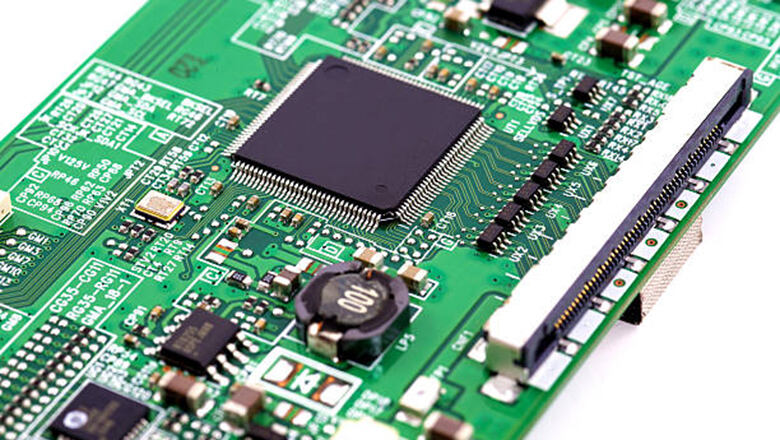
Reflow soldering technology serves as the fundamental process for modern high-quality PCB assembly production. This technique achieves electrical interconnection by accurately mounting surface mount devices(SMDs) onto designated pad locations on circuit boards. As the predominant method within the surface mount technology (SMT) system, reflow soldering demonstrates distinctive characteristics in applications involving miniaturized electronic components and high-density circuit designs.When compared with conventional wave soldering processes, reflow soldering exhibits remarkable process adaptability. Its flexibility accommodates diverse component configurations, while its system scalability addresses varying production capacity requirements.
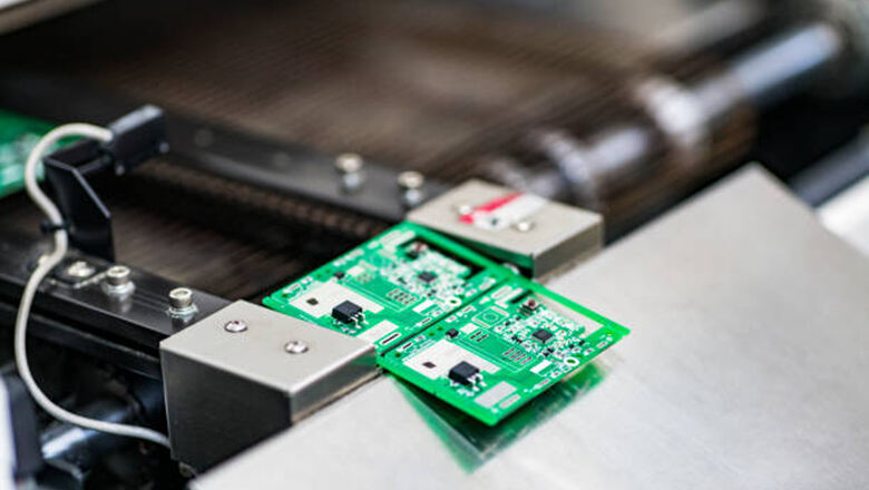
The reflow soldering process consists of three sequentially executed critical operational steps. First, operators need to accurately apply solder paste material to the designated pad areas on the circuit board. Specialized pick-and-place equipment then positions electronic components precisely onto the paste-coated locations according to programmed parameters. The component-populated circuit board subsequently enters a reflow oven with controlled temperature profiles to complete the soldering process, during which the solder paste material undergoes physical transformations of melting and solidification within the oven, ultimately forming reliable solder joints possessing both mechanical strength and electrical connectivity. This comprehensive soldering procedure constitutes the core process system of modern electronic assembly production lines. Its technical applications have fully expanded across both consumer electronics and industrial control sectors, with specific product categories encompassing portable devices like smartphones and industrial equipment such as automotive control systems.
The continuing trend of miniaturization in electronic devices and the increasing integration density of circuit boards are presenting new technical challenges to reflow soldering processes. Modern manufacturing must systematically address multiple typical soldering defects, including solder bridging, solder balling , cold solder joint, voiding defects, and thermal stress damage. For these categories of defects, specialized process improvement measures must be implemented. Manufacturers need to systematically conduct in-depth research on defect formation mechanisms and establish precise process control systems based on the research findings. The application of this technical management approach provides dual assurance for electronic assembly products: on one hand, it ensures a sufficiently high production yield rate during the manufacturing process, and on the other hand, it guarantees consistent and stable operation throughout the product's entire service life.
The Reflow Soldering Process in Surface Mount Technology (SMT)

The reflow soldering process can be summarized into several key stages. The preheat zone implements precise temperature control to achieve flux activation. The reflow zone facilitates metallurgical bonding of solder to form reliable solder joints. Each process stage exerts decisive influence on solder joint quality. All these elements collectively constitute the fundamental assurance for the overall reliability of circuit components.
1. Solder Paste Application
- Stencil Printing Process: Using stencils, solder paste is deposited onto selected pcb pads. The printing process must control the amount of solder paste deposited to avoid defects, including excessive solder (leading to bridging) or insufficient solder paste (causing incomplete solder joints).
- Paste Application Consistency: Advanced lines use automated solder paste inspection systems to monitor paste volume, shape, and deposition, immediately flagging any deviations.
2. Component Placement
- Pick-and-Place Machines: These automate the fast, precise placement of components onto freshly pasted pads, ensuring speed and accuracy across the pcb.
- Control of Placement: Well-tuned machines prevent component skewing and mitigate the risk of component misalignment.
3. Reflow Heating
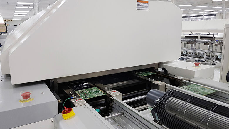
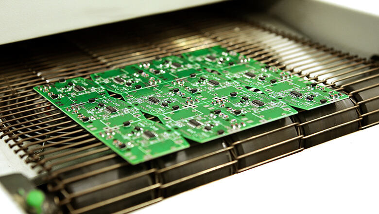
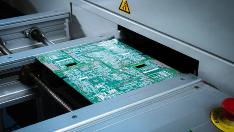
- Reflow Oven: The assembly passes through a multi-zone reflow oven where controlled, uniform heat melts the solder paste. Proper heating across the pcb ensures all joints solidify to create strong electrical and mechanical connections.
- Temperature Profiles: Reflow ovens are programmed with a specific temperature ramp-up, soak time, peak temperature, and cooling rate, all tailored to the specific assembly process and materials.
4. Cooling
- Uniform Heat Dissipation: Controlled cooling prevents thermal shock and ensures robust, void-free solder joints. Uneven cooling can promote stress, warping, or cracks.
5. Post-Assembly Inspection
- Automated and Manual Inspection: AOI, X-ray, and manual checks verify that solder has flowed and wetted correctly, and that no soldering defects (like solder bridges or solder balling) remain.
Common Challenges and Defects in Reflow Soldering

Welding technology continues to advance. Reflow soldering processes still face multiple common challenges. Unresolved issues will lead to quality problems in circuit board assemblies.
These manifest as overall product quality degradation or functional failures.
1. Solder Bridging
- Definition: Solder bridging occurs when excess solder forms an unintended electrical connection between two or more adjacent pads or leads.
- Why It Happens: Poor stencil design, excessive solder paste deposition, or incorrect oven settings can all result in this defect.
2. Solder Balling
- Definition: Tiny spheres of solder (solder balls) remain scattered across the pcb after reflow.
- Causes: Often due to moisture in the paste, rapid temperature ramp, or dirty boards/stencils.
3. Tombstoning
- Definition: A component stands on one end (“like Manhattan skyscrapers”) due to uneven heating or pad size discrepancies.
- Impact: Causes open circuits due to incomplete solder joint formation.
4. Cold Solder Joints
- Definition: Joint appears dull, grainy, or porous; often fails electrically or mechanically.
- Reasons: Low oven temperature, insufficient solder paste, or contaminated pad during reflow.
5. Voids and Incomplete Joints
- Voids within the solder joint undermine current carrying and heat dissipation capacity, especially on power and ground pads.
- Defect often caused by outgassing, poor paste selection, or inadequate reflow profiles.
6. Component Misalignment
- Pad during reflow may see components shift, causing functional failure and rework costs due to uneven surface tension or excessive vibration during the reflow process.
Summary Table: Common Defects and Causes
Defect |
Common Causes |
Solution Focus |
Solder bridging |
Excessive solder, poor stencil, uneven heat |
Stencil design, paste control |
Solder balling |
Moisture, contaminated boards, rapid ramp-up |
Paste storage, ramp optimization |
Cold solder joints |
Low temp, contamination, insufficient paste |
Oven calibration, surface prep |
Tombstoning |
Uneven pad heating, pad size |
Pad design, profile optimization |
Voids |
Outgassing, bad paste, poor heating |
Solder selection, profile tuning |
Root Causes Behind Soldering Defects

Addressing these challenges requires digging into root causes. Some major variables that frequently lead to defect formation:
1. Solder Paste Selection and Application
- Solder Paste Selection: The process involves evaluating alloy, particle size, and flux chemistry. Incorrect selections can lead to incomplete solder joints, excessive residue, or brittle connections.
- Solder Paste Application: The printing process must control the amount of solder dispensed. Automated solder paste inspection can dramatically reduce printing defects.
2. Stencil Design and Maintenance
- Aperture Shape & Size: Directly impacts deposition and thus the volume of solder paste. Bad design leads to excess (bridging) or insufficient solder (cold or incomplete joints).
- Maintenance and Cleaning: Dirty stencils reduce paste release uniformity, leading to print misalignments and bonding issues.
3. Reflow Oven Settings and Calibration
- Temperature Profile: Setting the right reflow profile to achieve uniform wetting and defect-free joints is vital.
- Calibration of the Reflow: Inconsistent or erratically programmed ovens cause uneven heat across the pcb, resulting in voids, warping, or joint failure.
4. PCB and Pad Design
- Pad Size and Layout: Pads that are too large/small or unevenly spaced can promote bridging and tombstoning.
- Thermal Relief and Vias: Adding thermal vias and balancing copper pour regions reduces the risk of cold solder joints and thermal shock.
5. Process Parameters and Environmental Conditions
- Humidity and Temperature: Uncontrolled conditions can lead to paste slumping, oxidation, and solder paste partially wets defects.
- Process in Surface Mount Technology: Modern SMT lines must track ambient conditions and adjust as necessary for consistent results.
Effective Solutions in Reflow Soldering
Solutions in reflow soldering target each root cause and are tuned to address the full range of process variables:
1. Controlling Solder Paste Volume and Application
- Use automated solder paste inspection systems after every print cycle.
- Regularly check stencil cleanliness and replace worn stencils.
- Match stencil aperture area ratio to pad size for consistent and reliable solder deposition.
2. Optimizing the Reflow Profile
- Use Real-Time Thermal Profilers: Place thermocouples across the pcb to gather actionable data for every area and component type. This ensures uniform heat distribution, avoiding local overheating or insufficient reflow, which could otherwise lead to defects like cold solder joints or weak adhesion.
- Gradual Temperature Ramp-Up: The reflow process should involve a controlled ramp, steady soak, targeted peak, and gradual cooldown. Quick spikes or improper dwell times can bring about defects caused by incomplete melting or uneven wetting—especially around thermal mass imbalances due to uneven component distribution.
- Tailor Oven Settings to Each Assembly: Every PCB design may demand unique oven settings due to differing copper distribution, component density, and board thickness. Fine-tuning process parameters and validating each batch preserves high-quality solder joints and minimizes common defects include solder bridges or voids.
3. Preventing Solder Bridging and Excessive Solder Deposition
Solder bridging is a typical defect in the soldering process. This phenomenon directly causes circuit shorts. Such short circuits represent significant quality risks in electronic assembly.
Key Prevention Measures:
- Stencil Optimization: Design stencil apertures to regulate the amount of solder paste accurately. From the printing process, manage paste application and paste deposits to combat excessive solder.
- Improve Solder Paste Release: Select stencils with nano-coatings or polished apertures and use the correct squeegee pressure. This ensures paste clears the stencil completely, reducing unwanted solder bridges.
- Automated Solder Paste Inspection: Deploy automated systems to monitor and reject any pcb assemblies with excessive solder or poor deposition, correcting the issue before reflow.
4. Reducing Voids, Cold Joints, and Incomplete Soldering
Voids within the solder joint reduce heat transfer.The formation of cold solder joint defects primarily stems from two typical causes: non-uniform temperature distribution during heating or insufficient solder paste deposition below process standards. Inadequate heating results in localized incomplete melting of solder material, while insufficient paste volume leads to weakened intermetallic bond strength. These process anomalies directly compromise the mechanical integrity of solder connections and substantially diminish their long-term operational reliability under field operating conditions.
Effective Solutions:
- Low-Voiding Solder Paste Selection: Newer pastes are engineered to reduce void formation under BGAs and QFNs, critical for high-current or thermal management designs.
- Profiling for Uniform Heating: Adjust the temperature profile to maximize uniform melting across the pcb without overheating low-mass areas. The right deposition and profile help prevent incomplete solder joints.
- Design for Assembly: Specify proper pad size and thermal vias to allow heat to reach every joint, especially under large, heat-dissipating parts.
5. Addressing Tombstoning, Balling, and Component Movement
Tombstoning and solder balling are often traced to uneven heat or incorrect paste/placement.
Key Strategies:
- Ensure pad symmetry and match the component termination for balanced solder flow.
- Balance temperature profiles during preheat and soaking phases.
- During double-sided circuit board assembly, manufacturing personnel should implement adhesive pre-fixing solutions for heavy and precision components. This pre-fixing procedure ensures all types of components maintain stable positioning before entering the reflow oven.
6. Ensuring Solder Paste and Stencil Maintenance
Reliable outcomes depend on maintenance and calibration:
- Stencil Cleaning Protocols: Regularly clean stencils to prevent dried solder paste from blocking apertures and affecting paste application quality.
- Reflow Equipment Calibration: Log and routinely calibrate reflow ovens and placement machines. This preserves accurate heating across the pcb and correct paste deposition cycle to cycle.
7. Leveraging Automated Inspection and Data
- Automated Solder Paste Inspection (SPI): Inline SPI checks every deposit on every board for volume, height, and location, catching potential defect before downstream processes.
- AOI and X-Ray: Use automated inspection to verify solder joint completeness, check for common challenges like insufficient solder, and spot hidden flaws.
Best Practices for Achieving Reliable Solder Joints

Manufacturing enterprises should establish stable production targets for high-quality solder joints and reliable PCB assembly. Production departments need to comprehensively integrate the following core optimization solutions into existing assembly processes. The systematic implementation of these technical measures can effectively enhance product consistency and process reliability.
- End-to-End Control of the Solder Process:
Document and monitor each reflow step, from solder paste selection to oven profile and inspection.
- Continuous Training and Improvement:
Enterprises should organize systematic skills training courses for operators. Manufacturing departments need to conduct specialized technical training based on IPC standards. Factories should establish regular process review mechanisms. These measures will significantly enhance the capability in defect detection and prevention.
Maintain controlled production area humidity and temperature to prevent issues from moisture in solder paste or extreme environmental swings.
- Implement Data-Driven Optimization:
Collect, review, and respond to trends in inspection data to uncover hidden issues—such as micro-bridging, incomplete solder joints, or batch-specific trends.
Inspection, Troubleshooting, and Repair Strategies
Manufacturing enterprises must first establish a complete and standardized production process system. They should subsequently develop systematic quality inspection standards while simultaneously formulating efficient rework handling solutions. These management measures collectively ensure the effective operation of the production system:
- Automated Solder Paste and Joint Inspection: Integrate SPI and AOI into your assembly process, enabling real-time alerts for problems like solder bridging, insufficient solder paste, or skewed placement.
- Root Cause Analysis: When a defect is found, trace its source: Was it excessive solder, incorrect thermal profiling, or placement drift?
- Repair and Rework Techniques: For recoverable defects, skilled repair techs can use heated air tools or localized reflow stations—always logging any work to track defect origins and rework rates.
- Feedback Loop: Addressing these challenges not only improves immediate yield but also prevents future similar issues.
Advanced Optimization: From Materials to Oven Calibration

Materials and Paste Selection Advances
- Solder Paste Engineering: Choose pastes that match your assembly’s requirements for slump, tack, and reflow characteristics—especially for fine-pitch or high-density PCB assemblies.
- Lead-Free Considerations: Carefully adjust reflow profiles for newer, higher-melting-point lead-free alloys to avoid defects stemming from insufficient melting.
Oven Technology and Predictive Maintenance
- Smart Ovens: Modern reflow ovens include sensors that map temperature in real time, alerting to drift or developing anomalies in temperature profile before they cause mass defects.
- Predictive Maintenance: Use machine learning and SPC data to schedule oven cleanings, fan replacements, and calibration before defects appear—even automating alerts for deviating yields or rising false-accept rates.
IoT and Smart Manufacturing
- Integrate reflow lines into factory-wide MES systems for full traceability, environmental monitoring, and automatic defect reporting.
- Cross-link pick-and-place, printing, reflow, and inspection data to get a holistic picture of your entire SMT line.
Frequently Asked Questions
Q: What’s the main difference between reflow soldering and wave soldering?
A: Reflow soldering melts solder paste only where components are mounted—supporting fine-pitch, double-sided, and high-density boards. Wave soldering passes the board over a molten solder wave, best for through-hole assembly and less effective for modern fine-pitch SMT work.
Q: Why do solder bridging and balling still occur even with automated inspection?
A: Even with automation, excessive solder, uneven pad sizes, dirty stencils, or imprecise oven programming can cause these common challenges if not corrected at the process root.
Q: How can I be sure my reflow profile is correct?
A: Optimize using thermal profilers, validate across the pcb, and sample multiple boards. Adjust your profile for each new design, especially when changing solder paste or major component layout.
Q: Does automated solder paste inspection eliminate all paste-related defects?
A: Automated inspection catches most paste volume and shape issues but must be paired with good stencil maintenance, correct paste selection, and environmental controls for best results.
Q: What should I do if I consistently see voids or incomplete solder joints?
A: Audit your paste quality, oven calibration, and check for contamination. Adjust dwell times and ramp rates, and switch to lower-voiding pastes if needed.
Conclusion: Mastering Reflow Soldering Challenges and Solutions
Conquering reflow soldering challenges and solutions is an ongoing journey. By understanding the common challenges in reflow—such as solder bridging occurs when excess solder is not managed, uneven heating across the pcb, or pad during reflow with insufficient solder—engineers and manufacturers can deploy effective solutions, from solder paste selection to optimizing the reflow profile.
Through careful control of stencil design, oven calibration, paste application, and continuous inspection, your team can consistently deliver high-quality solder joints, minimize the occurrence of defects, and achieve reliable, world-class PCB assemblies. Advanced analytics and smart manufacturing only strengthen your tools for success.
