The constant progress of technology has moved electronics toward devices that are smarter, faster, and more compact. The demand for these products has driven the development of high-density technologies that could be quickly assembled and reliably join the increasing complexity of modern circuits. Ball grid array (BGA) devices have emerged as a cornerstone solution, owing to their ability to maximize circuit density and enhance performance in PCB assembly.
Modern electronic manufacturing has widely adopted BGA components. This technology is utilized both in consumer electronics including smartphones and gaming devices, as well as in high-end sectors such as aerospace and medical electronics. Manufacturing enterprises must master soldering techniques for BGA components, possess operational capabilities for X-ray inspection systems, and be proficient in advanced rework techniques for BGA components. These professional technical skills hold significant value during the prototype development phase and are equally indispensable in mass production processes. Comprehensive mastery of this technical system ensures that final products meet performance standards.

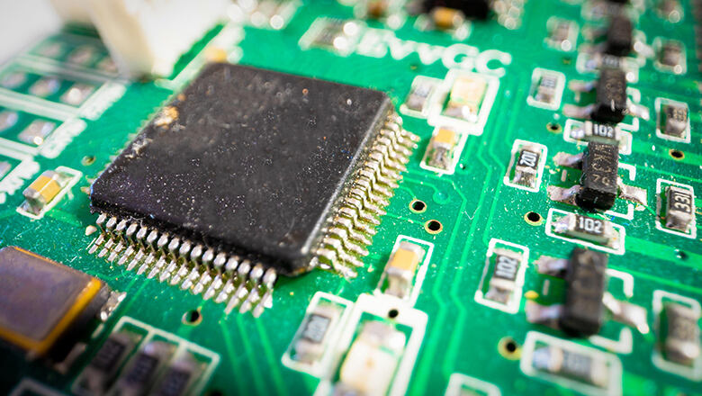
A ball grid array (BGA) is an integrated circuit packaging technology where solder balls are arranged in a grid pattern beneath the BGA device. During the assembly process these balls melt and form mechanical and electrical connections between the package and the PCB. Unlike traditional packages, BGA solder joints are hidden—making them inaccessible to simple visual inspection and increasing the reliance on advanced inspection technology like x-ray inspection.
Layer |
Function |
Inspection Technique |
Package substrate |
Houses integrated circuit |
Optical inspection (edge only) |
Solder balls |
Electrical/mechanical links |
X-ray inspection, Automated x-ray inspection |
PCB pads |
Soldered to a PCB |
Visual & electrical test |

The development of ball grid array technology was fueled by the need to increase I/O density and improve performance in electronic assemblies. As integrated circuit inside the package generated more heat and required more robust connections, the BGA became a pivotal advancement.
The shift toward BGA and PCB partnerships came from the need for devices that could handle high-speed performance, greater power, and more connections without enlarging the circuit board. This technological leap led to almost all processors, FPGAs, and high-speed memory being packaged as BGA ICs in the latest generations of electronic products.

BGA package soldering demands significantly higher technical requirements than conventional leaded packages. The process aims for complete consistency in solder ball placement. Key objectives include achieving precise heating temperature control. The procedure ultimately requires the formation of clean and void-free solder joints.
Variable |
Impact |
Solution |
Ball pitch |
Affects density, alignment needs |
Tighter = more challenging |
Soldering temperature |
Determines joint quality, risk of board warp |
Profile and monitor closely |
Solder paste amount |
Excess = bridging, Insufficient = open circuit |
Stencil design and SPI |
Placement accuracy |
Misalignment = solder bridge/defect |
Use of vision/alignment systems |
Reflow oven profile |
Controls wetting, avoids thermal shock |
Multi-zone ovens, use thermocouples |
Because BGA solder joints are hidden beneath the package, identifying a defect using only visual cues is virtually impossible. This makes x-ray inspection, along with other inspection techniques (optical inspection, electrical test), an essential part of the process.
1. Visual Inspection:
2. Optical Inspection (AOI):
4. Electrical Test:
5. Other Inspection Methods:
Inspection Method |
Detects |
Used to Inspect |
Limitation |
Visual & Optical Inspection |
Alignment, ball presence |
Placement/faulty BGA |
Can’t see hidden joints |
Automated X-ray Inspection (AXI) |
Voiding, bridging, opens |
Solder joint inspection |
Cost, operator skill |
Electrical Test |
Opens, shorts |
Circuit continuity |
Doesn’t detect all micro-defects |
IR/Acoustic Systems |
Cracks, overheating |
Post-reflow/field |
Specialized, partial data |
The evolution of inspection technology has brought about real-time 3D AXI, high-resolution x-ray systems, and software that can automatically flag when the temperature is too low during reflow or when a defect like insufficient solder is likely.

Even with excellent PCB and BGA design, various defects can occur during or after the soldering process. Understanding causes and prevention is key for robust circuits.
Defect Type |
Root Cause |
How to Avoid |
Solder Bridge |
Excess paste, misalignment |
Proper stencil, placement, inspection |
Insufficient Solder |
Incomplete paste printing, pad contamination |
SPI checks, clean pads |
Open Circuit |
Misaligned balls, insufficient heat, contamination |
Reprofile oven, calibrate placement |
Voiding in Solder Joints |
Fast ramp rate, contaminated paste |
Bake boards, stable process |
Head-in-Pillow |
Warped PCB or package, oxidation |
Bake components, control profile |
Cold Joint |
Low soldering temperature, poor wetting |
Validate reflow oven, check flux |
Pad Lift/Board Damage |
Overheating, aggressive rework |
Use proper rework station settings |
Tombstoning |
Uneven wetting, excessive pad temp |
Uniform temperature, adjust stencil |
When assembly or inspection reveals a defective solder joint or faulty BGA component, the bga rework process kicks in. A methodical approach is crucial to avoid further damage.
BGA Rework Station:
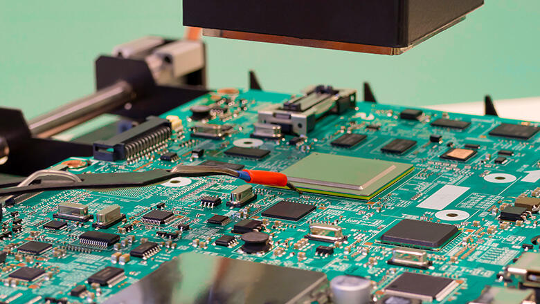
The core tool is a rework station designed for BGAs.
These rework stations come with precision temperature controls, vision systems for alignment, and specialized hot air nozzles or infrared heaters for locally heating the BGA component.
Hot Air Tool and IR Preheater:
Using a hot air tool allows safe removal of the defective part without disturbing adjacent solder joints.
IR preheater gently warms the circuit board to prevent warping or thermal shocks.
Vision Systems and Alignment:
Modern stations include cameras or microscopes to align the solder balls to pads with balls of solder precisely.
Reballing Tools:
For BGA devices that need to be reused, “reballing” replaces old, contaminated solder balls with new ones.
Solder Paste Printer or Mini Stencil:
For placing the right amount of solder for the new BGA.
Preparation
Inspect and confirm the defect and circuit to be repaired.
Remove moisture from the PCB and BGA with a pre-bake.
Removal
Use the rework station to locally heat the BGA component.
Once the solder balls have melted, lift the BGA with a vacuum tool.
Site Cleaning and Pad Inspection
Clean residual solder from PCB pads; inspect for pad lift or PCB damage.
New BGA Placement
For new BGA, apply solder paste to pads, use alignment guides for positioning.
Reflowing the Solder
Use the hot air tool or rework station controls to reflow the new solder balls and form connections between the BGA and PCB.
Final Inspection
Perform x-ray inspection, visual inspection, and electrical test as needed.
Q: Can manual soldering be used for BGA devices?
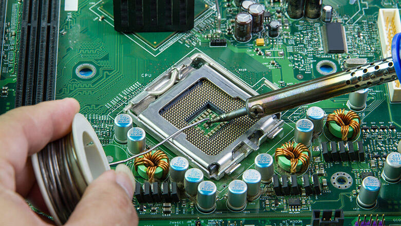
A: Manual soldering is generally not suitable for BGA assembly due to the hidden and fine-pitch nature of the solder joints. However, it plays a critical role in rework using special hot air nozzles and precise visual inspection.
Q: Is x-ray always needed for BGA inspection?
A: Yes, for production—since the solder joints are hidden under the package and cannot be assessed fully via visual or optical techniques.
Q: What are signs that a BGA solder process has failed?
A: Intermittent signals, no output, or device failure; confirmed by x-ray inspection or failed electrical tests.
Q: How do you avoid common BGA defects during reflow?
A: Correct oven profiling, careful stencil design, and routine inspection techniques minimize both obvious and subtle defects.
The development of ball grid array packaging has been pivotal in meeting the relentless demand for smaller, more powerful, and more reliable electronic devices. However, the solder joints of BGA devices—arranged in a grid pattern and hidden at the bottom of the package—demand sophisticated assembly, rework, and inspection techniques. From the use of reflow ovens and state-of-the-art bga rework stations to the necessity of advanced x-ray inspection, the full process demands attention to every detail.
Avoiding common BGA defects requires robust process controls and a commitment to using the right tools and inspection methods. The intersection of good design, expert soldering technique, precise inspection, and careful rework ensures that every high-density circuit board—and every integrated circuit inside the package—delivers on its promise of durability and performance.
Stay ahead in the ever-evolving world of PCB assembly—master BGA solder, keep inspection technology current, and invest in your team’s skills.