Professional PCB Stencils: Precision Engineering for Advanced Electronics Manufacturing

All Categories

stencil in pcb

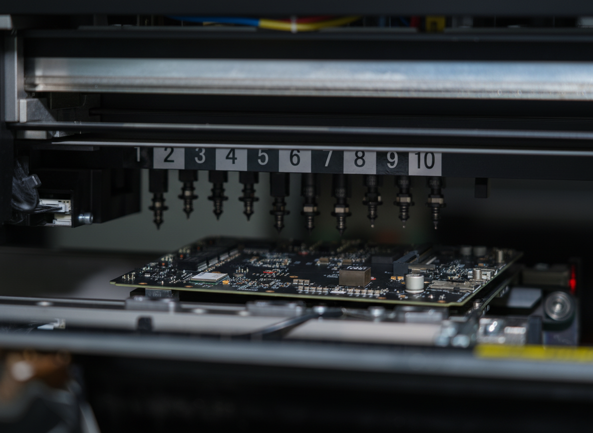
A PCB stencil is a precision-engineered tool essential in the surface mount technology (SMT) assembly process. This thin metal sheet, typically made from stainless steel, features carefully designed apertures that align perfectly with the PCB's solder pad positions. During the manufacturing process, the stencil is positioned over the circuit board, and solder paste is applied through these openings using a squeegee mechanism. The thickness of the stencil, usually ranging from 0.1mm to 0.2mm, plays a crucial role in determining the amount of solder paste deposited. Modern PCB stencils utilize advanced laser cutting technology to achieve precise aperture dimensions and clean edges, ensuring consistent solder paste deposition. The stencil design considers various factors including pad size, component pitch, and paste release characteristics. Nano-coating treatments can be applied to enhance paste release performance, particularly beneficial for fine-pitch applications. PCB stencils come in different types, including framed and frameless options, each suited to specific production requirements. The accuracy and quality of the stencil directly impact the reliability of solder joints and, consequently, the overall functionality of the assembled electronic device.

New Product Releases

PCB stencils offer numerous significant advantages in electronic manufacturing processes. First, they ensure precise and uniform solder paste deposition, which is crucial for achieving reliable solder joints. This consistency significantly reduces the risk of common assembly defects such as solder bridges or insufficient solder. The use of stencils also dramatically improves production efficiency by enabling simultaneous application of solder paste to multiple pads, substantially reducing the time required for the paste application process compared to manual methods. Modern stencil technologies incorporate advanced features like step-down areas for components of varying heights and special aperture designs for optimal paste release. The durability of stainless steel stencils ensures long-term reliability and repeated use without degradation in quality. Furthermore, stencils contribute to cost reduction by minimizing solder paste waste and reducing rework requirements due to paste application errors. The precision of laser-cut stencils allows manufacturers to work with increasingly miniaturized components and fine-pitch applications, keeping pace with the trend toward smaller electronic devices. Environmental benefits include reduced waste generation and lower energy consumption compared to alternative methods. Stencils also offer flexibility in manufacturing, as they can be quickly changed for different PCB designs, facilitating efficient production line changeovers. The quality control aspect is enhanced as stencils provide consistent, measurable paste deposits that can be easily monitored and adjusted as needed.

Latest News

What Are the Different Types of PCBs and Their Applications?

09

Oct

What Are the Different Types of PCBs and Their Applications?

Understanding Modern Printed Circuit Board Varieties Printed Circuit Boards (PCBs) form the backbone of modern electronics, serving as the foundation for countless devices we use daily. From smartphones to industrial machinery, different types of PCB...
View More
Why Choose PCB Solutions for Industrial Applications?

09

Oct

Why Choose PCB Solutions for Industrial Applications?

The Evolution of PCB Solutions in Modern Industrial Landscapes The industrial sector has witnessed a remarkable transformation with the integration of advanced PCB solutions into its core operations. From automated manufacturing facilities to sophist...
View More
How Are PCBs Manufactured? Key Steps and Processes Explained

09

Oct

How Are PCBs Manufactured? Key Steps and Processes Explained

Understanding the Complex Journey of Circuit Board Production PCB manufacturing has revolutionized the electronics industry, enabling the creation of increasingly sophisticated devices that power our modern world. From smartphones to medical equipmen...
View More
Why Choose Professional PCB Manufacturing Services?

09

Oct

Why Choose Professional PCB Manufacturing Services?

The Critical Role of Expert PCB Production in Modern Electronics In today's rapidly evolving electronics industry, the quality and reliability of printed circuit boards (PCBs) have become more crucial than ever. Professional PCB manufacturing service...
View More

Get a Free Quote

Our representative will contact you soon.
Email
Name
Company Name
Message
0/1000

stencil in pcb

Precision Engineering and Manufacturing

Precision Engineering and Manufacturing

PCB stencils represent the pinnacle of precision engineering in electronics manufacturing. The laser cutting process used in modern stencil production achieves aperture accuracy down to micrometers, essential for today's high-density circuit boards. This precision is maintained through sophisticated manufacturing controls, including temperature-controlled environments and automated inspection systems. The stencil's material composition, typically high-grade stainless steel, undergoes specific heat treatments to ensure dimensional stability and resistance to warping. Advanced surface finishing techniques, including electropolishing and nano-coating treatments, enhance the stencil's performance by improving paste release characteristics and extending operational life.
Versatility and Adaptability

Versatility and Adaptability

Modern PCB stencils demonstrate remarkable versatility in accommodating various PCB designs and component requirements. The ability to incorporate multiple thickness areas within a single stencil allows for optimal paste deposition for different component types. Manufacturers can specify custom aperture designs for unique component footprints, ensuring optimal solder paste volume for each application. The adaptability extends to different production volumes, from prototype runs to high-volume manufacturing, with options for both framed and frameless designs. The stencil's design can be quickly modified through computer-aided design systems, allowing rapid adaptation to new product requirements or design modifications.
Quality and Process Control

Quality and Process Control

PCB stencils play a crucial role in maintaining consistent quality in electronics assembly. The precise control over solder paste volume they provide is essential for achieving reliable solder joints and reducing defect rates. Advanced stencil designs incorporate features like anti-bridging apertures and optimized wall angles to prevent common assembly issues. The repeatability of the stencil printing process enables manufacturers to implement statistical process control methods, tracking and adjusting parameters to maintain optimal quality levels. Modern stencils also feature fiducial marks and positioning systems that ensure accurate alignment with the PCB, critical for fine-pitch components and complex assemblies.
Professional PCB Stencils: Precision Engineering for Advanced Electronics Manufacturing

Get a Free Quote

Our representative will contact you soon.
Email
Name
Company Name
Message
0/1000