printed circuit board design and fabrication
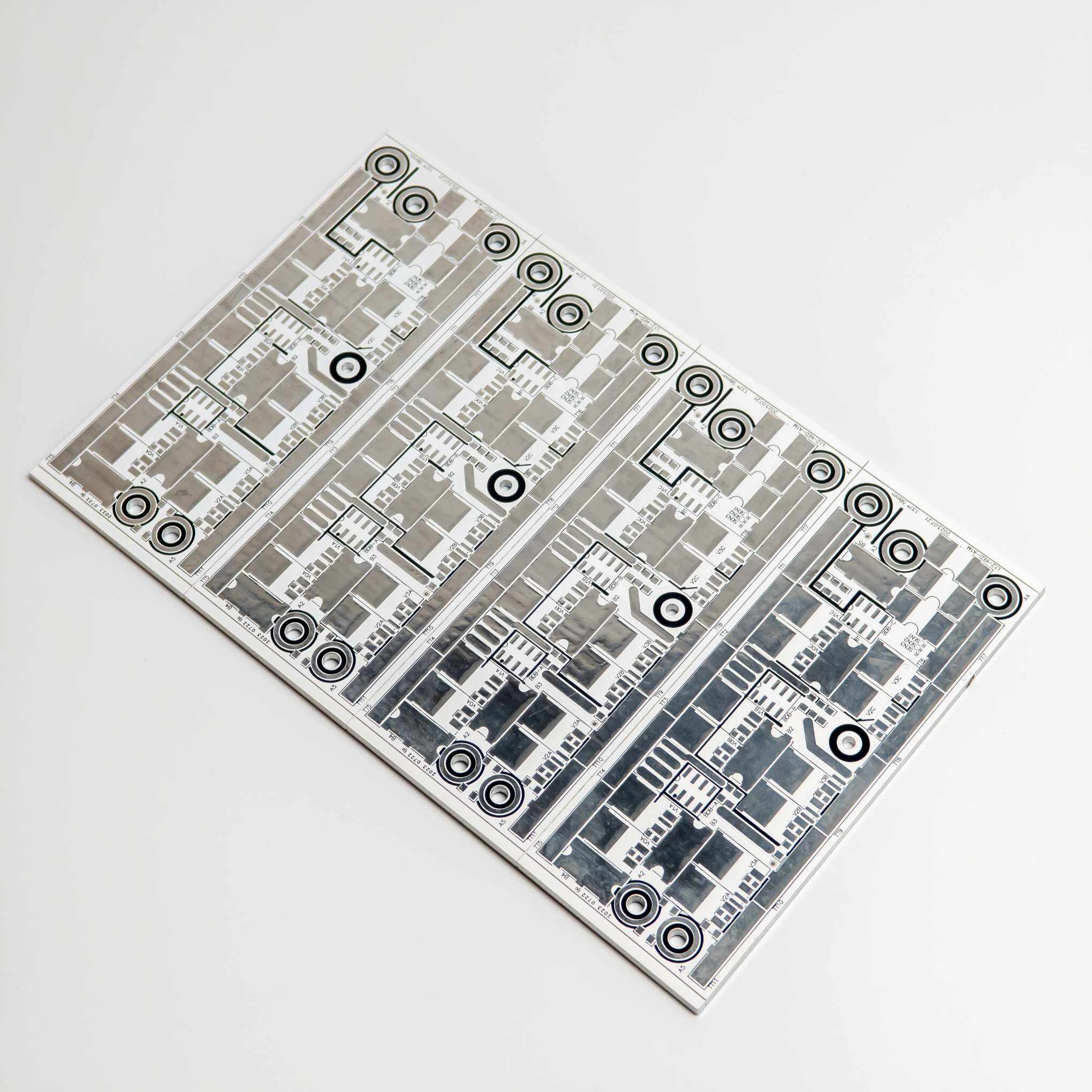
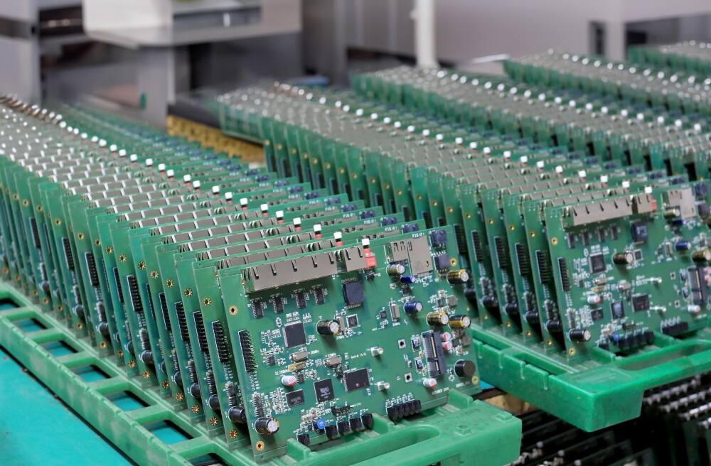
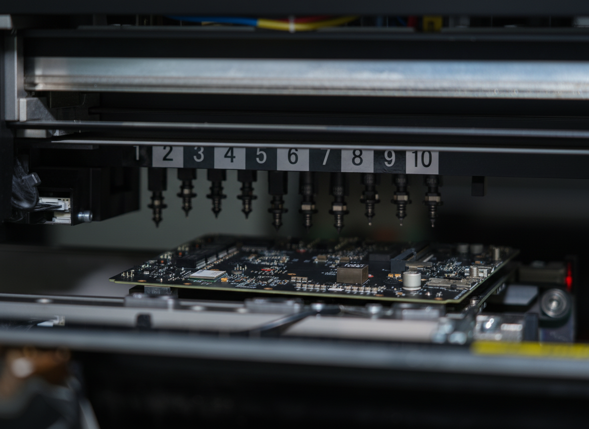
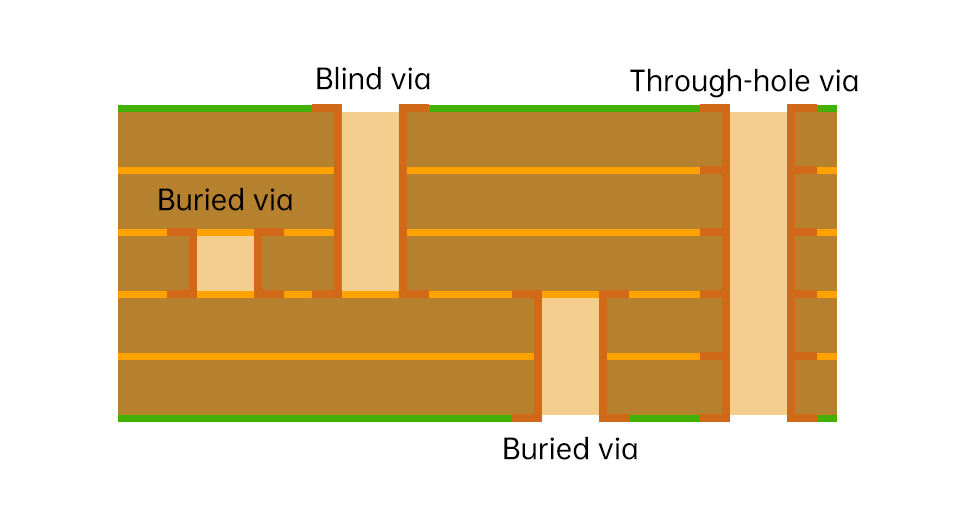
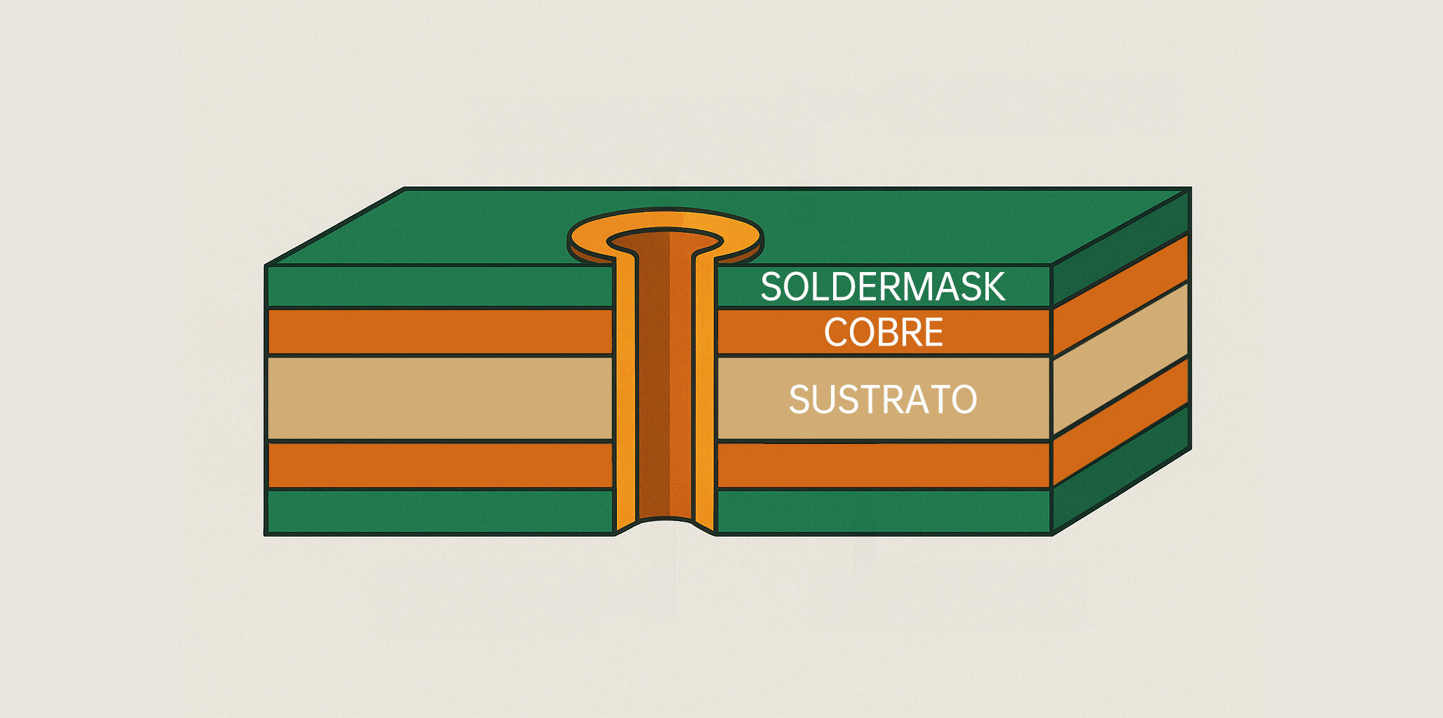
Printed circuit board (PCB) design and fabrication represents a cornerstone of modern electronics manufacturing, serving as the foundation for virtually all electronic devices. This sophisticated process involves creating a detailed layout of electrical connections and components on a non-conductive substrate. The design phase encompasses careful planning of circuit paths, component placement, and signal integrity analysis, while the fabrication process includes multiple steps such as substrate preparation, copper layering, photolithography, etching, and final assembly. Modern PCB design and fabrication utilizes advanced computer-aided design (CAD) software, enabling engineers to create complex multilayer boards with precise specifications. These boards can accommodate various components, from simple resistors to complex microprocessors, while maintaining optimal electrical performance and thermal management. The technology supports diverse applications across industries, including consumer electronics, aerospace, medical devices, and telecommunications. Contemporary PCB manufacturing processes incorporate automated quality control systems, ensuring consistent production quality and reliability. The integration of surface mount technology (SMT) and through-hole mounting methods allows for high-density component placement, making it possible to create increasingly compact and powerful electronic devices.