Advanced PCB Circuit Design: Innovative Solutions for Modern Electronics Manufacturing

All Categories

pcb circuit design

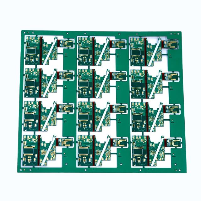
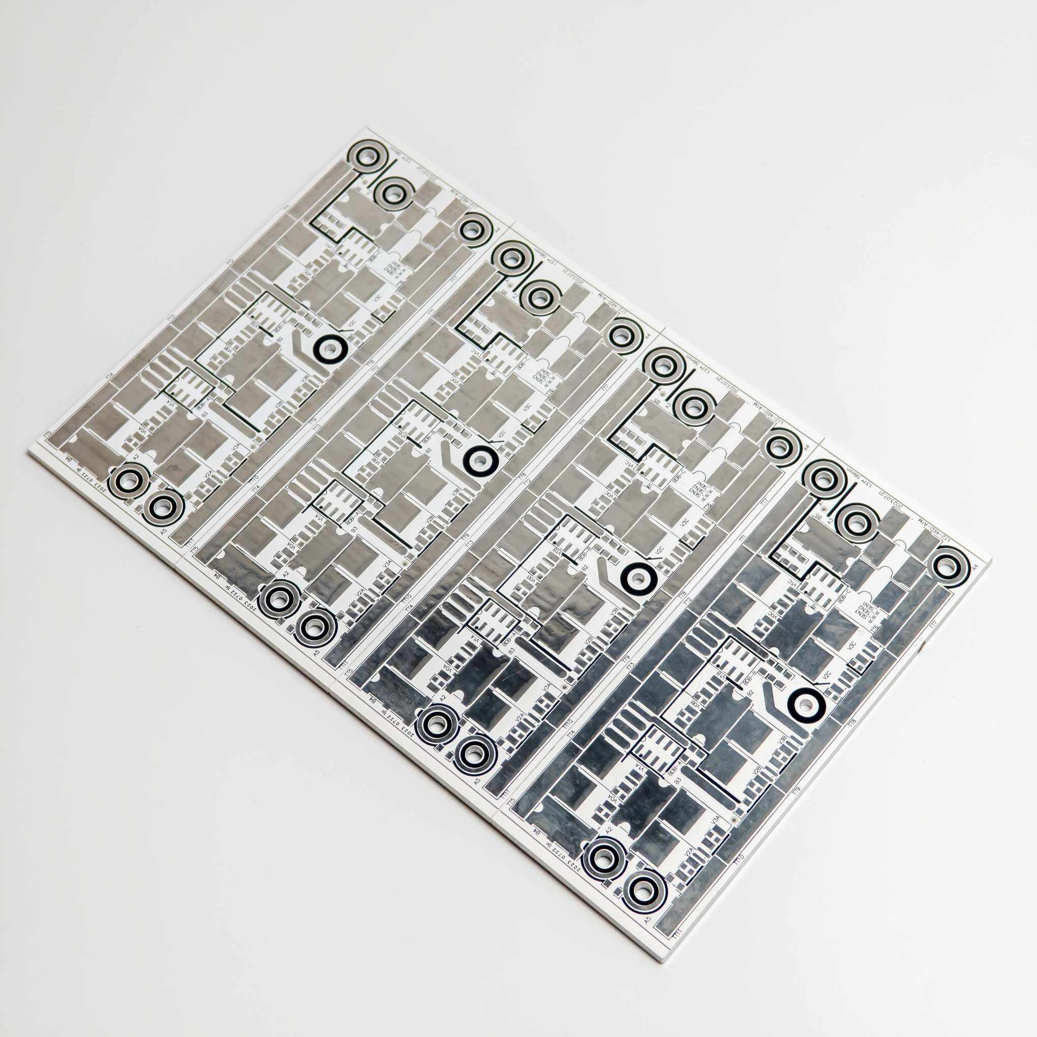
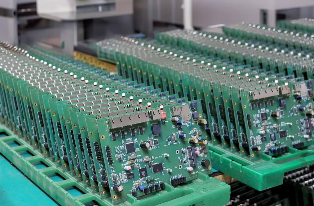
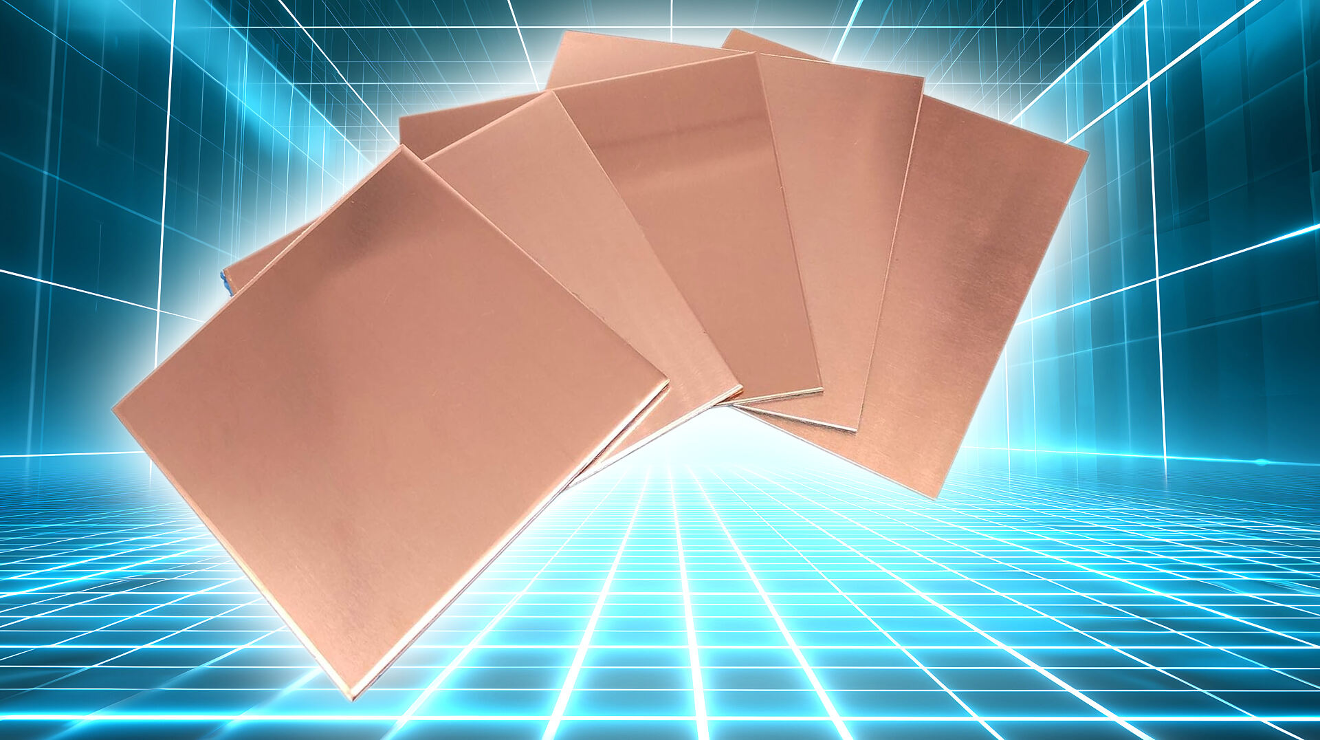
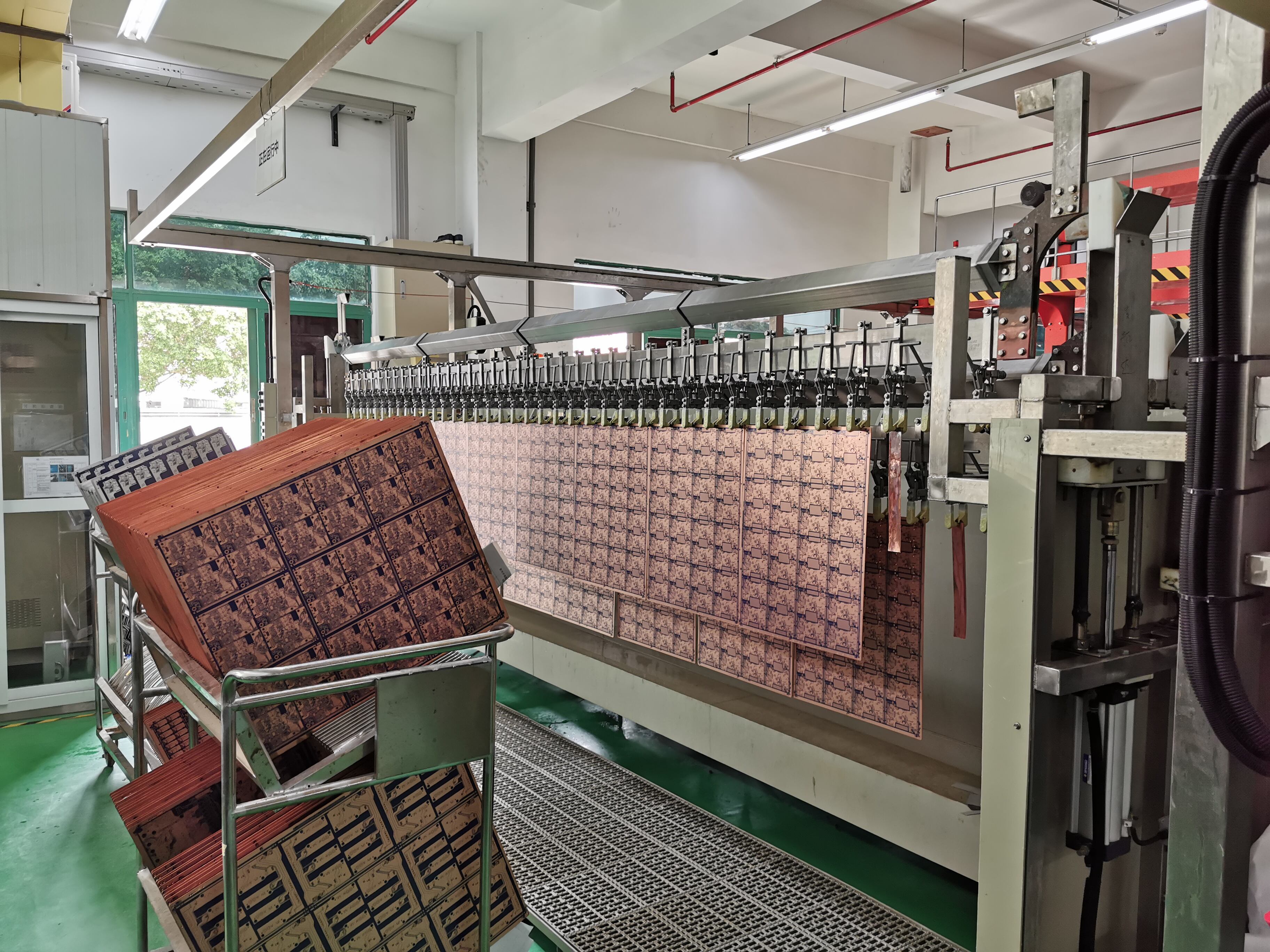
PCB circuit design represents a fundamental aspect of modern electronics manufacturing, encompassing the intricate process of creating printed circuit boards that serve as the backbone of electronic devices. This sophisticated design process involves mapping out complex electrical connections, component placements, and signal paths on a compact, layered substrate. The design incorporates multiple layers of conductive material, typically copper, separated by insulating layers, allowing for high-density component placement and efficient signal routing. Modern PCB circuit design utilizes advanced computer-aided design (CAD) software, enabling engineers to create precise layouts, perform signal integrity analysis, and optimize thermal management. The design process considers crucial factors such as electromagnetic compatibility, power distribution, and manufacturing constraints. These designs support various technologies, from simple single-layer boards to complex multilayer configurations capable of supporting high-speed digital circuits, RF applications, and mixed-signal systems. The versatility of PCB circuit design makes it essential in industries ranging from consumer electronics and automotive systems to medical devices and aerospace applications.

Popular Products

PCB circuit design offers numerous compelling advantages that make it indispensable in modern electronics manufacturing. First, it provides exceptional reliability through consistent, automated production processes that minimize human error and ensure repeatable results. The design methodology enables significant space optimization, allowing complex circuits to fit into compact form factors while maintaining optimal performance. Cost-effectiveness is another major benefit, as mass production of PCBs reduces per-unit costs significantly compared to point-to-point wiring methods. The structured nature of PCB design also facilitates easier troubleshooting and maintenance, with clear component layouts and standardized connection patterns. Heat dissipation is greatly improved through proper component placement and the use of thermal management techniques integrated into the design phase. Signal integrity is enhanced through controlled impedance routing and minimized electromagnetic interference, crucial for high-speed applications. The modular nature of PCB designs allows for easier upgrades and modifications, reducing time-to-market for new product iterations. Manufacturing efficiency is increased through automated assembly processes, with precise component placement and soldering. Additionally, PCB designs can incorporate various test points and debugging features, making quality control and maintenance more straightforward. The scalability of PCB production means designs can be easily adapted for different production volumes, from prototypes to mass manufacturing.

Tips And Tricks

What Are the Different Types of PCBs and Their Applications?

09

Oct

What Are the Different Types of PCBs and Their Applications?

Understanding Modern Printed Circuit Board Varieties Printed Circuit Boards (PCBs) form the backbone of modern electronics, serving as the foundation for countless devices we use daily. From smartphones to industrial machinery, different types of PCB...
View More
What Problems Can Happen in PCB Circuit Boards and How to Solve Them?

09

Oct

What Problems Can Happen in PCB Circuit Boards and How to Solve Them?

Understanding Common PCB Circuit Board Issues and Their Solutions PCB circuit boards are the backbone of modern electronics, serving as the foundation for countless devices we use daily. From smartphones to industrial machinery, these intricate compo...
View More
How Are PCBs Manufactured? Key Steps and Processes Explained

09

Oct

How Are PCBs Manufactured? Key Steps and Processes Explained

Understanding the Complex Journey of Circuit Board Production PCB manufacturing has revolutionized the electronics industry, enabling the creation of increasingly sophisticated devices that power our modern world. From smartphones to medical equipmen...
View More
Why Choose Professional PCB Manufacturing Services?

09

Oct

Why Choose Professional PCB Manufacturing Services?

The Critical Role of Expert PCB Production in Modern Electronics In today's rapidly evolving electronics industry, the quality and reliability of printed circuit boards (PCBs) have become more crucial than ever. Professional PCB manufacturing service...
View More

Get a Free Quote

Our representative will contact you soon.
Email
Name
Company Name
Message
0/1000

pcb circuit design

Advanced Multi-layer Technology

Advanced Multi-layer Technology

Modern PCB circuit design excels in multi-layer technology, revolutionizing electronic device capabilities. This sophisticated approach allows for complex routing solutions by utilizing multiple conductive layers separated by insulating material. The technology enables significantly higher component density while maintaining signal integrity through controlled impedance traces and proper ground planes. Engineers can implement advanced features such as buried vias and blind vias, optimizing space usage and reducing electromagnetic interference. The multi-layer approach also facilitates better power distribution, crucial for high-performance devices, while maintaining thermal management efficiency. This technology supports the integration of different types of circuits, from high-speed digital to sensitive analog components, on the same board while minimizing cross-talk and interference.
Automated Design and Verification

Automated Design and Verification

The integration of advanced CAD tools in PCB circuit design has transformed the development process, offering unprecedented accuracy and efficiency. These sophisticated software solutions provide real-time design rule checking, ensuring compliance with manufacturing constraints and industry standards. Automated routing algorithms optimize signal paths while maintaining proper clearances and minimizing signal degradation. The design tools include powerful simulation capabilities for analyzing signal integrity, power distribution, and thermal performance before physical production. This significantly reduces development cycles and prototyping costs while ensuring higher first-pass success rates. The automated verification process includes comprehensive checks for manufacturing feasibility, assembly requirements, and regulatory compliance.
Enhanced Manufacturing Efficiency

Enhanced Manufacturing Efficiency

PCB circuit design incorporates numerous features that streamline the manufacturing process, resulting in higher production efficiency and quality. The design process includes considerations for automated assembly equipment, with proper component spacing and orientation for pick-and-place machines. Fiducial marks are strategically placed to ensure accurate alignment during assembly, while test points are integrated for automated testing procedures. The designs include proper documentation and manufacturing files in standardized formats, facilitating smooth communication with manufacturing partners. Surface finish selections and solder mask specifications are optimized for specific applications and manufacturing processes, ensuring reliable solder joints and component attachment. This comprehensive approach to manufacturing-aware design results in higher yields and reduced production costs.
Advanced PCB Circuit Design: Innovative Solutions for Modern Electronics Manufacturing

Get a Free Quote

Our representative will contact you soon.
Email
Name
Company Name
Message
0/1000