Via Annular Ring Technology: Enhancing PCB Reliability and Performance

All Categories

via annular ring

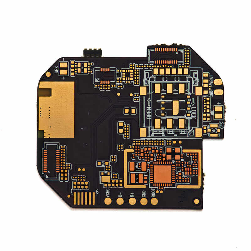
A via annular ring is a crucial element in printed circuit board (PCB) design, consisting of a copper area that surrounds a drilled hole or via on a PCB. This conductive ring serves as a vital connection point between different layers of the circuit board, ensuring proper electrical continuity and mechanical stability. The annular ring's primary function is to provide sufficient copper for reliable connections while accommodating manufacturing tolerances during the drilling and plating processes. The size and dimensions of via annular rings are carefully calculated based on several factors, including the drill size, manufacturing capabilities, and design requirements. In modern PCB manufacturing, via annular rings play a critical role in maintaining signal integrity, especially in high-speed digital circuits where precise impedance control is essential. They also contribute significantly to the overall reliability of the PCB by providing adequate mechanical strength to prevent delamination and ensuring proper copper plating during the manufacturing process. The technology behind via annular rings has evolved to accommodate increasingly complex PCB designs, with manufacturers now capable of producing smaller rings while maintaining reliability, thus enabling higher component density and more sophisticated circuit designs.

New Product Releases

Via annular rings offer numerous practical benefits that make them indispensable in modern PCB design and manufacturing. First, they provide enhanced mechanical strength at connection points, reducing the risk of copper separation and ensuring long-term reliability of the PCB. This increased durability translates to longer product life and fewer field failures. Second, via annular rings enable better electrical conductivity between PCB layers, resulting in improved signal integrity and reduced signal loss. This is particularly important in high-frequency applications where signal quality is paramount. The presence of properly sized annular rings also facilitates easier inspection and quality control during manufacturing, as technicians can visually verify proper alignment and connection integrity. From a manufacturing perspective, via annular rings provide crucial tolerance allowances that accommodate slight misalignments during the drilling process, significantly improving manufacturing yield rates. They also enhance the thermal management capabilities of the PCB by providing additional copper area for heat dissipation. For designers, via annular rings offer flexibility in routing options and help maintain consistent impedance control throughout the board. Additionally, they contribute to better plating distribution during the manufacturing process, ensuring uniform copper thickness and reliable electrical connections. The technology also supports the trend toward miniaturization in electronics, as modern manufacturing techniques allow for smaller yet highly reliable annular rings.

Tips And Tricks

What Are the Different Types of PCBs and Their Applications?

09

Oct

What Are the Different Types of PCBs and Their Applications?

Understanding Modern Printed Circuit Board Varieties Printed Circuit Boards (PCBs) form the backbone of modern electronics, serving as the foundation for countless devices we use daily. From smartphones to industrial machinery, different types of PCB...
View More
Why Choose PCB Solutions for Industrial Applications?

09

Oct

Why Choose PCB Solutions for Industrial Applications?

The Evolution of PCB Solutions in Modern Industrial Landscapes The industrial sector has witnessed a remarkable transformation with the integration of advanced PCB solutions into its core operations. From automated manufacturing facilities to sophist...
View More
How Are PCBs Manufactured? Key Steps and Processes Explained

09

Oct

How Are PCBs Manufactured? Key Steps and Processes Explained

Understanding the Complex Journey of Circuit Board Production PCB manufacturing has revolutionized the electronics industry, enabling the creation of increasingly sophisticated devices that power our modern world. From smartphones to medical equipmen...
View More
Why Choose Professional PCB Manufacturing Services?

09

Oct

Why Choose Professional PCB Manufacturing Services?

The Critical Role of Expert PCB Production in Modern Electronics In today's rapidly evolving electronics industry, the quality and reliability of printed circuit boards (PCBs) have become more crucial than ever. Professional PCB manufacturing service...
View More

Get a Free Quote

Our representative will contact you soon.
Email
Name
Company Name
Message
0/1000

via annular ring

Enhanced Reliability and Durability

Enhanced Reliability and Durability

The via annular ring's design significantly enhances the overall reliability and durability of printed circuit boards through multiple mechanisms. The additional copper area surrounding the via provides crucial mechanical support, preventing common failure modes such as copper lifting or delamination under thermal stress or mechanical strain. This enhanced structural integrity is particularly valuable in applications where the PCB may be subjected to vibration, thermal cycling, or mechanical stress. The larger contact area created by the annular ring also ensures better electrical connectivity, reducing the likelihood of connection failures over time. This improved reliability translates directly to longer product lifespans and reduced maintenance requirements, making it especially valuable in critical applications where failure is not an option.
Manufacturing Process Optimization

Manufacturing Process Optimization

Via annular rings play a crucial role in optimizing the PCB manufacturing process by providing necessary tolerances for drilling operations. The carefully calculated ring size accommodates potential misalignments during drilling while ensuring sufficient copper remains for reliable connections. This built-in tolerance significantly improves manufacturing yield rates by reducing the number of rejected boards due to misaligned or improperly formed vias. The technology also facilitates better plating processes, as the additional copper area provides improved adhesion for the plating material and ensures more uniform plating distribution. These manufacturing benefits ultimately lead to more consistent quality and lower production costs, making via annular rings a cost-effective solution for PCB production.
Signal Integrity and Performance

Signal Integrity and Performance

The implementation of via annular rings significantly enhances signal integrity and overall circuit performance in modern PCB designs. The optimized copper geometry around vias helps maintain consistent impedance control, which is crucial for high-speed digital circuits and RF applications. The additional copper area also provides better current handling capabilities, making it possible to design more robust power distribution networks. In high-frequency applications, properly designed annular rings help minimize signal reflections and losses, contributing to better signal quality and reduced electromagnetic interference. This improved signal performance is essential in modern electronic devices where data rates continue to increase and signal integrity requirements become more stringent.
Via Annular Ring Technology: Enhancing PCB Reliability and Performance

Get a Free Quote

Our representative will contact you soon.
Email
Name
Company Name
Message
0/1000