pcb production and assembly
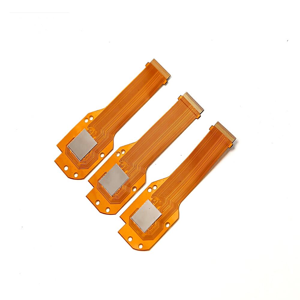
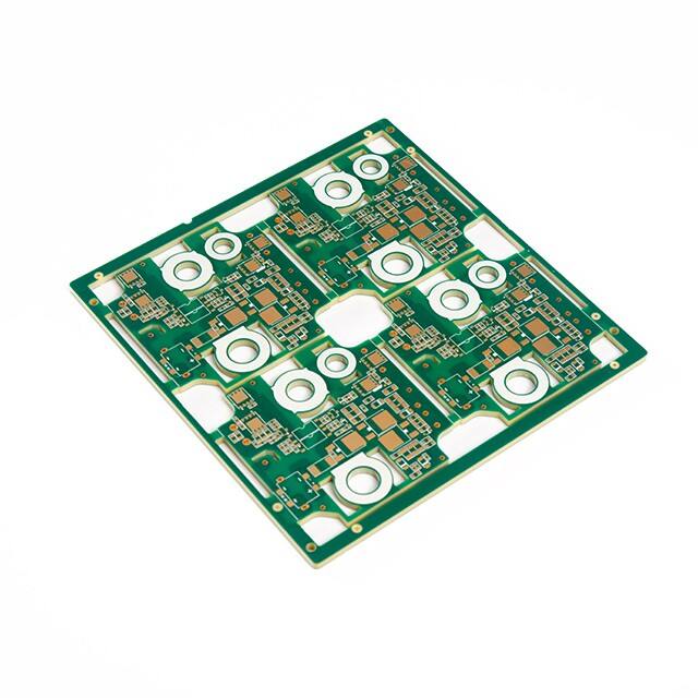
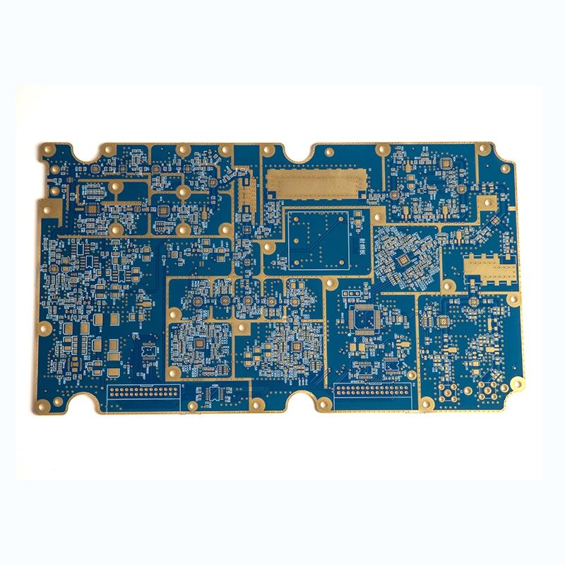
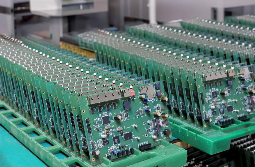
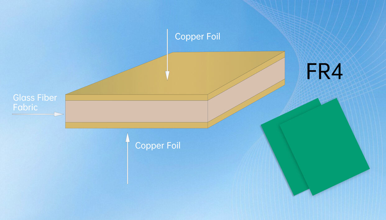
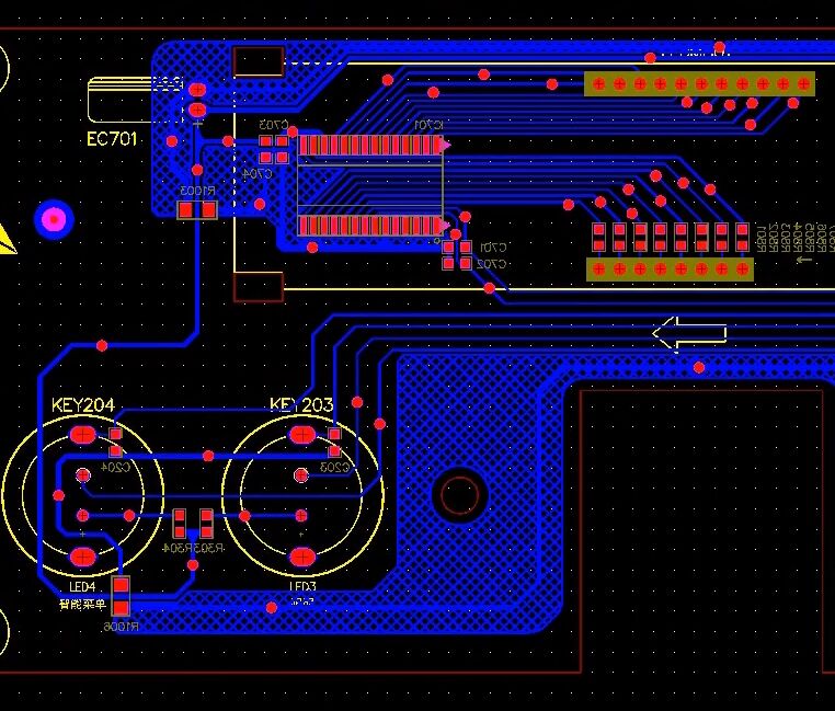
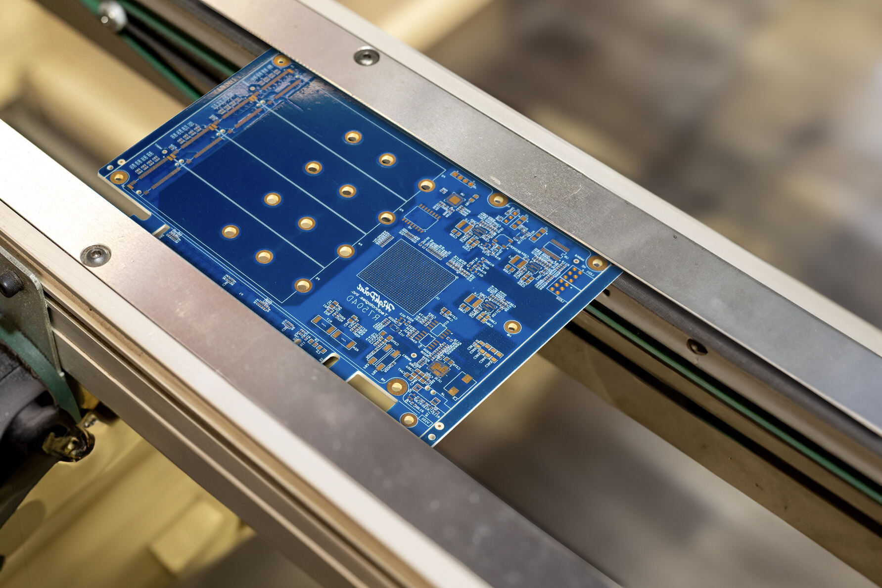
PCB production and assembly represents a critical manufacturing process that transforms electronic designs into functional circuit boards. This sophisticated process combines cutting-edge technology with precision engineering to create the backbone of modern electronic devices. The manufacturing begins with design verification, followed by the creation of multiple layers of copper-clad substrate material. These layers undergo precise etching to form intricate circuit patterns, which are then laminated together under controlled pressure and temperature. The assembly phase incorporates advanced surface-mount technology (SMT) and through-hole mounting techniques to place and secure components. Quality control measures, including automated optical inspection (AOI) and X-ray inspection, ensure each board meets exact specifications. The process accommodates various board types, from single-layer to complex multilayer designs, supporting applications ranging from consumer electronics to aerospace technology. Modern PCB production facilities utilize automated equipment for component placement, achieving placement accuracies down to micrometers while maintaining high throughput rates. This process integrates thermal management considerations, impedance control, and signal integrity requirements to ensure optimal performance in the final product.