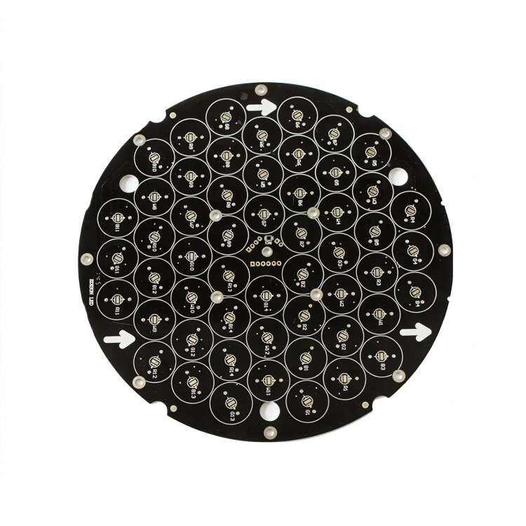
blind & buried vias
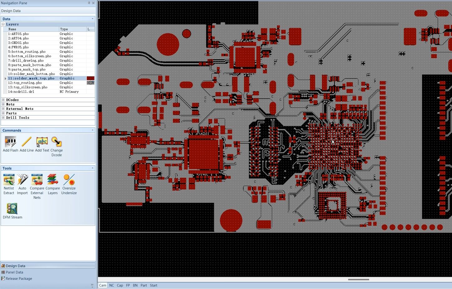
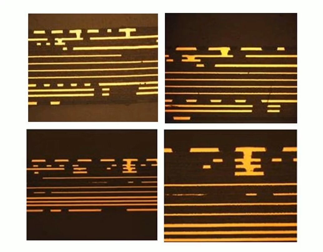
Blind and buried vias are essential components in modern printed circuit board (PCB) design, representing advanced interconnection technologies that enable complex multilayer circuit configurations. Blind vias connect an outer layer to one or more inner layers without extending through the entire board, while buried vias connect internal layers without being visible from the outside. These sophisticated interconnection methods allow for increased circuit density and improved signal integrity in multilayer PCBs. The technology enables designers to create more compact electronic devices while maintaining optimal performance. Blind and buried vias are particularly valuable in high-density interconnect (HDI) applications, where space optimization is crucial. They facilitate the development of smaller, more efficient electronic devices by allowing for more sophisticated routing options and better use of available board space. The implementation of these via types requires precise manufacturing processes, including laser drilling and sequential lamination, ensuring reliable connections between different PCB layers. Their use has become increasingly important in modern electronics, particularly in smartphones, tablets, and other portable devices where space optimization is essential while maintaining high performance and reliability standards.